10
LT3027
3027fa
APPLICATIO S I FOR ATIO
WUUU
Output Capacitance and Transient Response
The LT3027 regulator is designed to be stable with a wide
range of output capacitors. The ESR of the output capaci-
tor affects stability, most notably with small
capacitors. A minimum output capacitor of 1µF with an
ESR of 3 or less is recommended to prevent oscilla-
tions. The LT3027 is a micropower device and output
transient response will be a function of output capaci-
tance. Larger values of output capacitance decrease the
peak deviations and provide improved transient response
for larger load current changes. Bypass capacitors, used
to decouple individual components powered by the
LT3027, will increase the effective output capacitor value.
With larger capacitors used to bypass the reference (for
low noise operation), larger values of output capacitors
are needed. For 100pF of bypass capacitance, 2.2µF of
output capacitor is recommended. With a 330pF bypass
capacitor or larger, a 3.3µF output capacitor is recom-
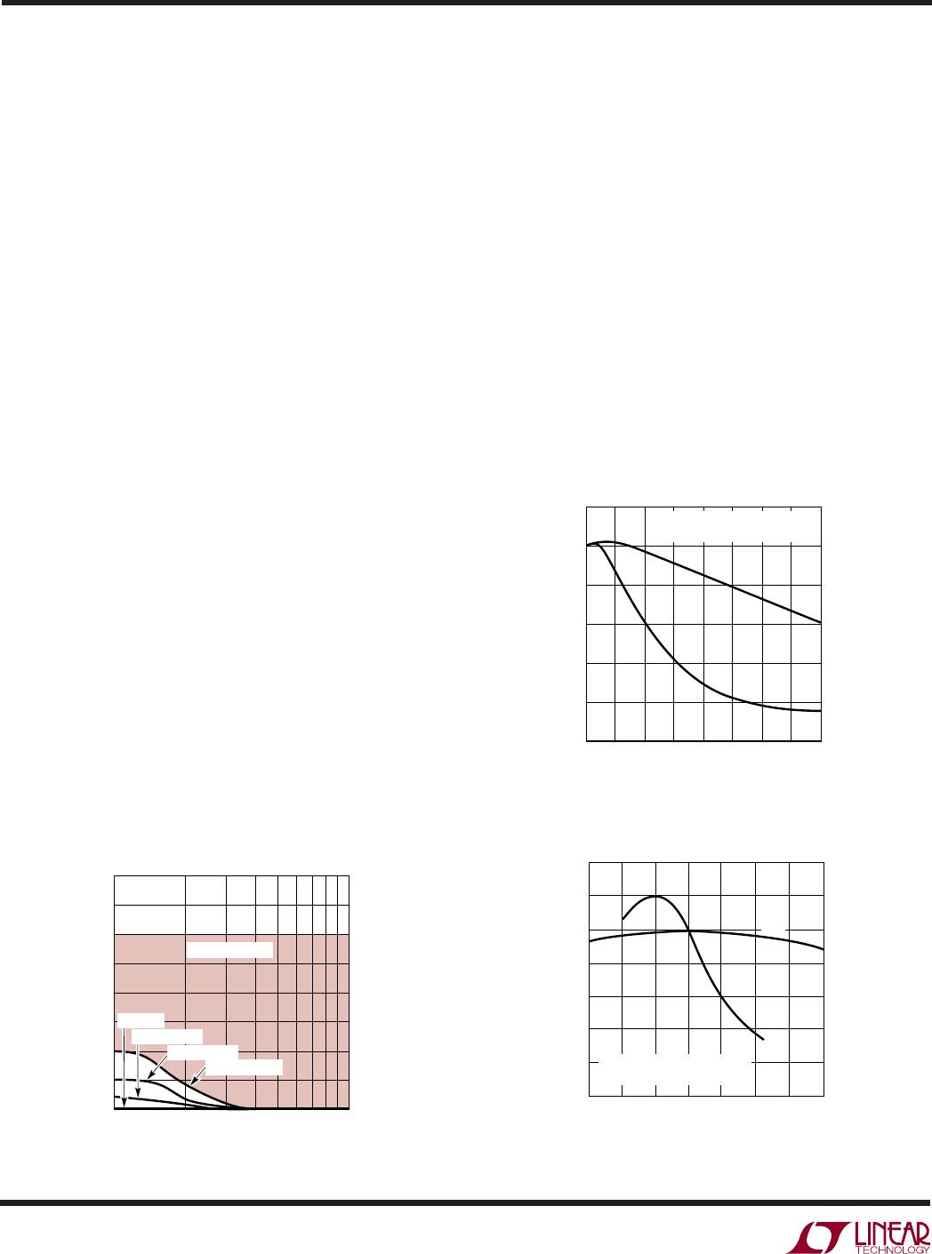
mended. The shaded region of Figure 2 defines the region
over which the LT3027 regulator is stable. The minimum
ESR needed is defined by the amount of bypass capaci-
tance used, while the maximum ESR is 3.
Extra consideration must be given to the use of ceramic
capacitors. Ceramic capacitors are manufactured with a
variety of dielectrics, each with different behavior across
temperature and applied voltage. The most common di-
electrics used are specified with EIA temperature charac-
teristic codes of Z5U, Y5V, X5R and X7R. The Z5U and Y5V
dielectrics are good for providing high capacitances in a
small package, but they tend to have strong voltage and
temperature coefficients as shown in Figures 3 and 4.
When used with a 5V regulator, a 16V 10µF Y5V capacitor
can exhibit an effective value as low as 1µF to 2µF for the
DC bias voltage applied and over the operating tempera-
ture range. The X5R and X7R dielectrics result in more
stable characteristics and are more suitable for use as the
output capacitor. The X7R type has better stability across
temperature, while the X5R is less expensive and is
available in higher values. Care still must be exercised
when using X5R and X7R capacitors; the X5R and X7R
codes only specify operating temperature range and maxi-
mum capacitance change over temperature. Capacitance
change due to DC bias with X5R and X7R capacitors is
better than Y5V and Z5U capacitors, but can still be
significant enough to drop capacitor values below appro-
priate levels. Capacitor DC bias characteristics tend to
improve as component case size increases, but expected
capacitance at operating voltage should be verified.
Figure 2. Stability
OUTPUT CAPACITANCE (µF)
1
ESR ()
4.0
3.5
3.0
2.5
2.0
1.5
1.0
0.5
0
310
3027 F02
245
6
78
9
STABLE REGION
C
BYP
= 330pF
C
BYP
= 100pF
C
BYP
= 0
C
BYP
> 3300pF
Figure 4. Ceramic Capacitor Temperature Characteristics
Figure 3. Ceramic Capacitor DC Bias Characteristics
TEMPERATURE (°C)
–50
40
20
0
–20
–40
–60
–80
100
25 75
3027 F04
–25 0
50 100 125
Y5V
CHANGE IN VALUE (%)
X5R
BOTH CAPACITORS ARE 16V,
1210 CASE SIZE, 10µF
DC BIAS VOLTAGE (V)
CHANGE IN VALUE (%)
3027 F03
20
0
–20
–40
–60
–80
100
0
4
8
10
26
12
14
X5R
Y5V
16
BOTH CAPACITORS ARE 16V,
1210 CASE SIZE, 10µF
11
LT3027
3027fa
For continuous normal conditions, the maximum junction
temperature rating of 125°C must not be exceeded. It is
important to give careful consideration to all sources of
thermal resistance from junction to ambient. Additional
heat sources mounted nearby must also be considered.
For surface mount devices, heat sinking is accomplished
by using the heat spreading capabilities of the PC board
and its copper traces. Copper board stiffeners and plated
through-holes can also be used to spread the heat gener-
ated by power devices.
The following tables list thermal resistance for several
different board sizes and copper areas. All measurements
were taken in still air on 3/32" FR-4 board with one ounce
copper.
Table 1. MSE Package, 10-Lead MSOP
COPPER AREA THERMAL RESISTANCE
TOPSIDE* BACKSIDE BOARD AREA (JUNCTION-TO-AMBIENT)
2500mm
2
2500mm
2
2500mm
2
40°C/W
1000mm
2
2500mm
2
2500mm
2
45°C/W
225mm
2
2500mm
2
2500mm
2
50°C/W
100mm
2
2500mm
2
2500mm
2
62°C/W
*Device is mounted on topside.
Table 2. DD Package, 10-Lead DFN
COPPER AREA THERMAL RESISTANCE
TOPSIDE* BACKSIDE BOARD AREA (JUNCTION-TO-AMBIENT)
2500mm
2
2500mm
2
2500mm
2
40°C/W
1000mm
2
2500mm
2
2500mm
2
45°C/W
225mm
2
2500mm
2
2500mm
2
50°C/W
100mm
2
2500mm
2
2500mm
2
62°C/W
*Device is mounted on topside.
The thermal resistance juncton-to-case (θ
JC
), measured
at the Exposed Pad on the back of the die is 10°C/W for the
10-lead MS package and 3°C for the 10-lead DFN package.
Calculating Junction Temperature
Example: Given an output voltage on the first channel of
3.3V, an output voltage of 2.5V on the second channel, an
input voltage range of 4V to 6V, output current ranges of
0mA to 100mA for the first channel and 0mA to 50mA for
the second channel, with a maximum ambient temperature
of 50°C, what will the maximum junction temperature be?
Voltage and temperature coefficients are not the only
sources of problems. Some ceramic capacitors have a
piezoelectric response. A piezoelectric device generates
voltage across its terminals due to mechanical stress,
similar to the way a piezoelectric accelerometer or
microphone works. For a ceramic capacitor the stress
can be induced by vibrations in the system or thermal
transients. The resulting voltages produced can cause
appreciable amounts of noise, especially when a ceramic
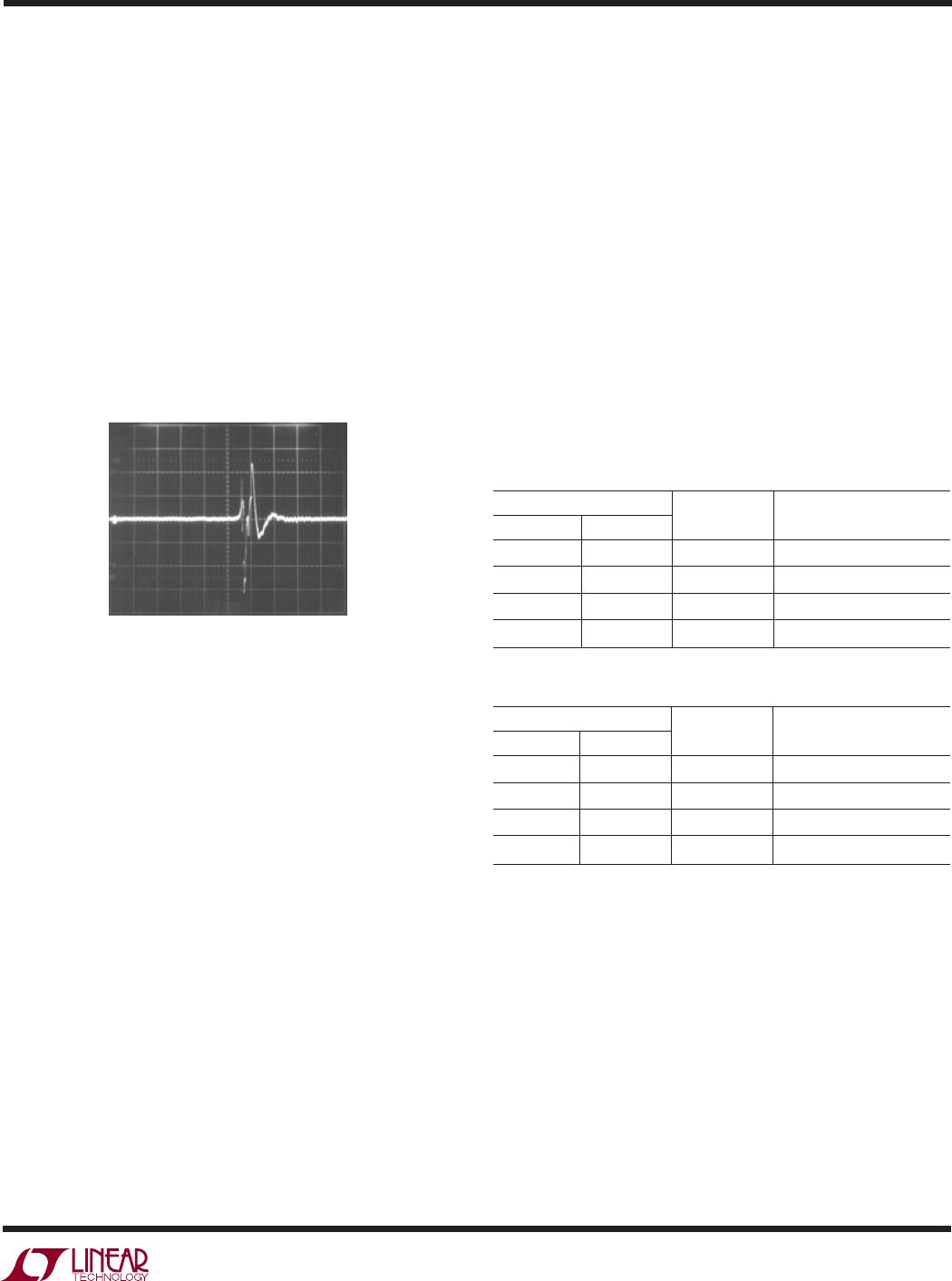
capacitor is used for noise bypassing. A ceramic capaci-
tor produced Figure 5’s trace in response to light tapping
from a pencil. Similar vibration induced behavior can
masquerade as increased output voltage noise.
APPLICATIO S I FOR ATIO
WUUU
Thermal Considerations
The power handling capability of the device will be limited
by the maximum rated junction temperature (125°C). The
power dissipated by the device will be made up of two
components (for each channel):
1. Output current multiplied by the input/output voltage
differential: (I
OUT
)(V
IN
– V
OUT
), and
2. GND pin current multiplied by the input voltage:
(I
GND
)(V
IN
).
The ground pin current can be found by examining the
GND Pin Current curves in the Typical Performance
Characteristics section. Power dissipation will be equal to
the sum of the two components listed above. Power
dissipation from both channels must be considered dur-
ing thermal analysis.
The LT3027 regulator has internal thermal limiting de-
signed to protect the device during overload conditions.
100ms/DIV 3027 F05
V
OUT
500µV/DIV
Figure 5. Noise Resulting from Tapping on a Ceramic Capacitor
C
OUT
= 10µF
C
BYP
= 0.01µF
I
LOAD
= 100mA
12
LT3027
3027fa
The power dissipated by each channel of the device will be
equal to:
I
OUT(MAX)
(V
IN(MAX)
– V
OUT
) + I
GND
(V
IN(MAX)
)
where (for the first channel):
I
OUT(MAX)
= 100mA
V
IN(MAX)
= 6V
I
GND
at (I
OUT
= 100mA, V
IN
= 6V) = 2mA
so:
P1 = 100mA(6V – 3.3V) + 2mA(6V) = 0.28W
and (for the second channel):
I
OUT(MAX)
= 50mA
V
IN(MAX)
= 6V
I
GND
at (I
OUT
= 50mA, V
IN
= 6V) = 1mA
so:
P2 = 50mA(6V – 2.5V) + 1mA(6V) = 0.18W
The thermal resistance will be in the range of 40°C/W to
60°C/W depending on the copper area. So the junction
temperature rise above ambient will be approximately
equal to:
(0.28W + 018W)(60°C/W) = 27.8°C
The maximum junction temperature will then be equal to
the maximum junction temperature rise above ambient
plus the maximum ambient temperature or:
T
JMAX
= 50°C + 27.8°C = 77.8°C
Protection Features
The LT3027 regulator incorporates several protection fea-
tures which makes it ideal for use in battery-powered cir-
cuits. In addition to the normal protection features asso-
ciated with monolithic regulators, such as current limiting
and thermal limiting, the devices are protected against
reverse input voltages and reverse voltages from output to
input.
Current limit protection and thermal overload protection are
intended to protect the device against current overload
conditions at the output of the device. For normal opera-
tion, the junction temperature should not exceed 125°C.
The input of the device will withstand reverse voltages of
APPLICATIONS INFORMATION
WUU
U
20V. Current flow into the device will be limited to less than
1mA (typically less than 100µA) and no negative voltage will
appear at the output. The device will protect both itself and
the load. This provides protection against batteries which
can be plugged in backward.
The output of the LT3027 can be pulled below ground
without damaging the device. If the input is left open circuit
or grounded, the output can be pulled below ground by 20V.
The output will act like an open circuit; no current will flow
out of the pin. If the input is powered by a voltage source,
the output will source the short-circuit current of the de-
vice and will protect itself by thermal limiting. In this case,
grounding the SHDN pins will turn off the device and stop
the output from sourcing the short-circuit current.
The ADJ pins can be pulled above or below ground by as
much as 7V without damaging the device. If the input is left
open circuit or grounded, the ADJ pins will act like an open
circuit when pulled below ground and like a large resistor
(typically 100k) in series with a diode when pulled above
ground.
In situations where the ADJ pins are connected to a resis-
tor divider that would pull the pins above their 7V clamp
voltage if the output is pulled high, the ADJ pin input cur-
rent must be limited to less than 5mA. For example, a re-
sistor divider is used to provide a regulated 1.5V output from
the 1.22V reference when the output is forced to 20V. The
top resistor of the resistor divider must be chosen to limit
the current into the ADJ pin to less than 5mA when the ADJ
pin is at 7V. The 13V difference between output and ADJ
pin divided by the 5mA maximum current into the ADJ pin
yields a minimum top resistor value of 2.6k.
In circuits where a backup battery is required, several dif-
ferent input/output conditions can occur. The output volt-
age may be held up while the input is either pulled to ground,
pulled to some intermediate voltage or is left open circuit.
When the IN pins of the LT3027 are forced below the cor-
responding OUT pins or the OUT pins are pulled above the
IN pins, input current will typically drop to less than 2µA.
This can happen if the input of the device is connected to
a discharged (low voltage) battery and the output is held
up by either a backup battery or a second regulator circuit.
The state of the SHDN pins will have no effect on the reverse
output current when the output is pulled above the input.
LT3027EMSE#PBF

Mfr. #:
Manufacturer:
Analog Devices / Linear Technology
Description:
LDO Voltage Regulators 2x 100mA, L Drop, L N, uP Reg w/ Indepen
Lifecycle:
New from this manufacturer.
Delivery:
DHL FedEx Ups TNT EMS
Payment:
T/T Paypal Visa MoneyGram Western Union