3
Pin Descriptions
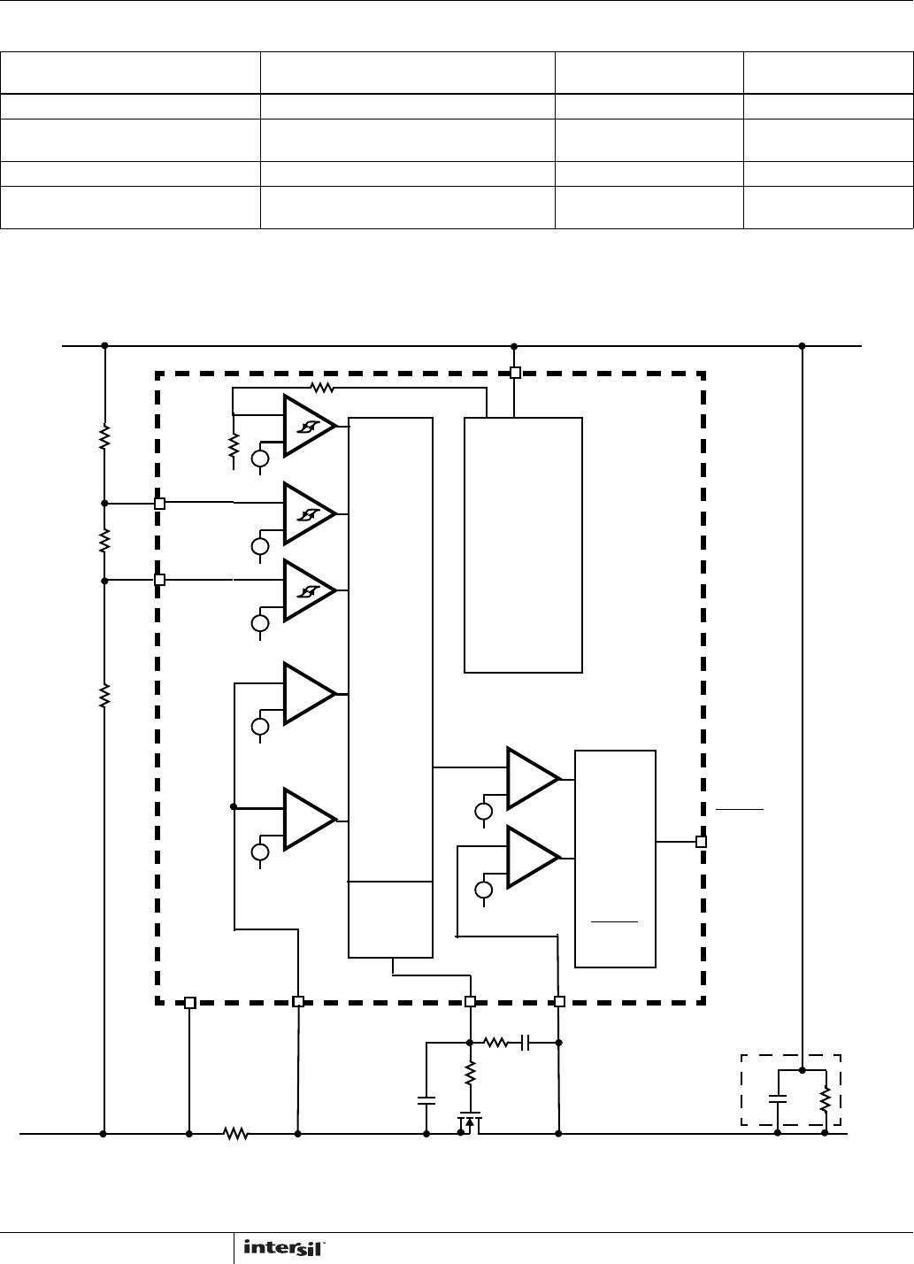
PWRGD (ISL6141; L Version) Pin 1
This digital output is an open-drain pull-down device. During
start-up the DRAIN and GATE voltages are monitored with
two separate comparators. The first comparator looks at the
DRAIN pin voltage compared to the internal V
PG
reference
(V
PG
is nominal 1.3V); this measures the voltage drop across
the external FET and sense resistor. When the DRAIN to V
EE
voltage drop is less than 1.3V, the first of two conditions
required for the power to be considered good are met. In
addition, the GATE voltage monitored by the second
comparator must be within approximately 2.5V of its normal
operating voltage (13.6V). When both criteria are met the
PWRGD
output will transition from high to low, enabling a
power module in some applications. The output is latched in
the low state until any of the signals that shut off the GATE
occur (Over-Voltage, Under-Voltage, Under-Voltage Lock-Out,
Over-Current Time-Out, or powering down). Any of these
conditions will re-set the latch and the PWRGD
output will
transition from low to high indicating power is no longer good.
In this case the output pull-down device shuts off, and the pin
becomes high impedance. Typically an external pull-up of
some kind is used to pull the pin high (many brick regulators
have a pull-up function built in).
PWRGD (ISL6151; H Version) Pin 1 - This digital
output is used to provide an active high signal to enable an
external module. The Power Good comparators are the
same as described above, but the active state of the output
is reversed (reference Figure 33).
If the latch is reset (GATE turns off), the internal DMOS
device (Q3) is turned off, and Q2 (NPN) turns on to clamp
the output one diode drop above the DRAIN voltage to
produce a logic low.
Once the latch is set (both DRAIN and GATE are normal), the
DMOS device (Q3) turns on and sinks current to V
EE
through
a 6.2K resistor. The base of Q2 is clamped to V
EE
to turn it
off. If the external pull-up current is high enough (>1mA, for
example), the voltage drop across the resistor will be large
enough to produce a logic high output (in this example, 1mA *
6.2k = 6.2V) and enable the external module.
Note that for all H versions, although this is a digital pin
functionally, the logic high level is determined by the external
pull-up device, and the power supply to which it is
connected; the IC will not clamp it below the V
DD
voltage.
Therefore, if the external device does not have its own
clamp, or if it would be damaged by a high voltage, an
external clamp might be necessary.
OV (Over-Voltage) Pin 2 - This analog input compares the
voltage on the pin to an internal voltage reference of 1.255V
(nominal). When the input goes above the reference (low to
high transition) an Over-Voltage condition is detected and
the GATE pin is immediately pulled low to shut off the
external FET. The built in 25mV hysteresis will keep the
GATE off until the OV pin drops below 1.230V, which is the
nominal high to low threshold. A typical application will use
an external resistor divider from V
DD
to V
EE
to set the OV
level as desired. A three-resistor divider can be used to set
both OV and UV trip points.
UV (Under-Voltage) Pin 3 - This analog input compares the
voltage on the pin to an internal comparator with a built in
hysteresis of 135mV. When the UV input goes below the
nominal reference (high to low transition) voltage of 1.120V,
the GATE pin is immediately pulled low to shut off the
external FET. Since the comparator has a built in 135mV
hysteresis the GATE will remain off until the UV pin rises
above a 1.255V low to high threshold. A typical application
will use an external resistor divider from V
DD
to V
EE
to set
the UV level as desired. A three-resistor divider can be used
to set both OV and UV trip points.
The UV pin is also used to reset the Over-Current latch. The
pin must be cycled below 1.120V (nominal) and then above
1.255V (nominal) to clear the latch and initiate a normal
power-up sequence.
V
EE
Pin 4 - This is the most negative supply voltage, such
as in a -48V system. Most of the other signals are
referenced relative to this pin, even though it may be far
away from what is considered a GND reference.
SENSE Pin 5 - This analog input monitors the voltage drop
across the external sense resistor (between SENSE and
V
EE
) to determine if the current exceeds the programmed
Over-Current trip point, equal to 50mV / Rsense. If the load
current exceeds the Over-Current threshold, the circuit will
regulate the current to maintain the nominal voltage drop
(50mV) across the sensing resistor R1 (Rsense). If current is
limited for more than 600s, the Over-Current shutdown
(also called electronic circuit breaker) will quickly turn off the
FET and latch the GATE pin off.
A Hard Fault comparator is employed to detect and respond
quickly to severe short circuits. The threshold of this
comparator is set approximately four times higher (210mV)
than the Over-Current trip point. When its threshold is
exceeded the GATE is immediately (10s typical) shut off,
the timer is reset, and a single retry (soft start) is attempted
before latching the GATE off (assuming the fault remains).
During the retry, if the fault disappears prior to the Over-
Current Time-Out period (600s) the FET will remain on as
normal. If the GATE is latched off, the user must either
toggle the UV pin below then above its threshold, or reduce
the supply voltage below the V
DD
UVLO trip point and then
above it. This will clear the latch and initiate a normal power-
up sequence.
ISL6141, ISL6151