Data Sheet ADV202
Rev. D | Page 31 of 40
PLL
The ADV202 uses the PLL_HI and PLL_LO direct registers to
configure the PLL. Any time the PLL_LO register is modified,
the host must wait at least 20 µs before reading or writing to any
other register. If this delay is not implemented, erratic behavior
could result.
The PLL can be programmed to have any possible final
multiplier value as long as
• JCLK > 50 MHz and < 150 MHz (144-lead version).
• JCLK > 50 MHz and < 135 MHz (144-lead version).
• JCLK > 50 MHz and < 115 MHz (121-lead version).
• HCLK < 108 MHz (144-lead, 150 MHz version).
• HCLK < 100 MHz (144-lead, 135 MHz version).
• HCLK < 81 MHz (121-lead version).
• JCLK ≥ 2 × VCLK for single-component input.
• JCLK ≥ 2 × VCLK for YCrCb [4:2:2] input.
• In JDATA mode (JDATA), JCLK must be 4 × MCLK or
higher.
• For de-interlaced modes, JCLK must be ≥ 4 × MCLK.
• The maximum burst frequency for external DMA modes is
≤0.36 JCLK.
• For MCLK frequencies greater than 50 MHz, the input
clock divider must be enabled, that is, IPD set to 1.
• IPD cannot be enabled for MCLK frequencies below 20 MHz.
To achieve the lowest power consumption, an MCLK frequency
of 27 MHz is recommended for a standard definition CCIR656
input. The PLL circuit is recommended to have a multiplier of 3.
This sets JCLK and HCLK to 81 MHz.
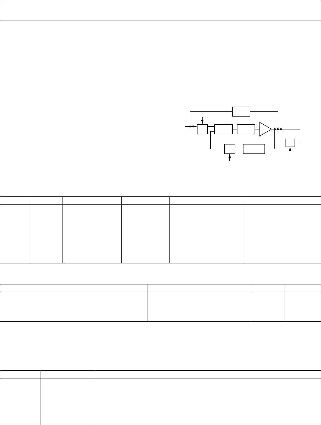
04723-009
LPF
PHASE
DETECT
VCO
JCLK
HCLK
2
HCLKD
PLLMULT 2
LFB
2
IPD
BYPASS
MCLK
Figure 23. PLL Architecture and Control Functions
Table 21. Recommended PLL Register Settings
IPD LFB PLLMULT HCLKD HCLK JCLK
0 0 N 0 N × MCLK N × MCLK
0 0 N 1 N × MCLK/2 N × MCLK
0 1 N 0 2 × N × MCLK 2 × N × MCLK
0 1 N 1 N × MCLK 2 × N × MCLK
1 0 N 0 N × MCLK/2 N × MCLK/2
1 0 N 1 N × MCLK/4 N × MCLK/2
1 1 N 0 N × MCLK N × MCLK
1 1 N 1 N × MCLK/2 N × MCLK
Table 22. Recommended Values for PLL_HI and PLL_LO Registers
Video Standard CLKIN Frequency on MCLK PLL_HI PLL_LO
SMPTE125M or ITU-R.BT656 (NTSC or PAL) 27 MHz 0x0008 0x0004
SMPTE293M (525p) 27 MHz 0x0008 0x0004
ITU-R.BT1358 (625p) 27 MHz 0x0008 0x0004
SMPTE274M (1080i) 74.25 MHz 0x0008 0x0084
HARDWARE BOOT
The boot mode can be configured via hardware using the CFG pins or via software (see the ADV202 User’s Guide). The first boot mode
after power-up is set by the CFG pins. Only Boot Mode 2, Boot Mode 4, and Boot Mode 6, described in Table 23, are available via hardware.
Table 23. Hardware Boot Modes
Boot Mode Settings Description
Hardware Boot
Mode 2
CFG[1] tied high,
CFG[2] tied low
No-Boot Host Mode. ADV202 does not boot, but all internal registers and memory are accessible
through normal host I/O operations.
For details, see the ADV202 User’s Guide and the Getting Started with the ADV202 application note.
Hardware Boot
Mode 4
CFG[1] tied low,
CFG[2] tied high
SoC Boot Mode.
Hardware Boot
Mode 6
CFG[1] and CFG[2]
tied high
Reserved.