LT3080
10
3080fc
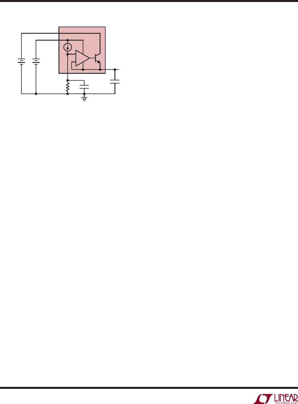
Figure 1. Basic Adjustable Regulator
+
LT3080
IN
V
CONTROL
V
CONTROL
OUT
3080 F01
SET
C
OUT
R
SET
V
OUT
C
SET
+
V
IN
+
Output Voltage
The LT3080 generates a 10µA reference current that flows
out of the SET pin. Connecting a resistor from SET to
ground generates a voltage that becomes the reference
point for the error amplifier (see Figure 1). The reference
voltage is a straight
multiplication of the SET pin current
and the value of the resistor. Any voltage can be generated
and there is no minimum output voltage for the regulator.
A minimum load current of 1mA is required to maintain
regulation regardless of output voltage. For true zero
voltage output operation, this 1mA load current must be
returned to a negative supply voltage.
With the low level current used to generate the reference
voltage, leakage paths to or from the SET pin can create
errors in the reference and output voltages. High quality
insulation should be used (e.g., Teflon, Kel-F); cleaning
of all insulating surfaces to remove fluxes and other resi-
dues will probably be required. Surface coating may be
necessary to provide a moisture barrier in high humidity
environments.
Board leakage can be minimized by encircling the SET
pin and circuitry with a guard ring operated at a potential
close to itself; the guard ring should be tied to the OUT
pin. Guarding both sides of the circuit board is required.
Bulk leakage reduction depends on the guard ring width.
Ten nanoamperes of leakage into or out of the SET pin and
associated circuitry creates a 0.1% error in the reference
voltage. Leakages of this magnitude, coupled with other
sources of leakage, can cause significant offset voltage
and reference drift, especially over the possible operating
temperature range.
If guardring techniques are used, this bootstraps any
stray capacitance at the SET pin. Since the SET pin is
a high impedance node, unwanted signals may couple
into the SET pin and cause erratic behavior. This will
be most noticeable when operating with minimum
output capacitors at full load current. The easiest way
to remedy this is to bypass the SET pin with a small
amount of capacitance from SET to ground, 10pF to
20pF is sufficient.
Stability and Output Capacitance
The LT3080 requires an output capacitor for stability. It
is designed to be stable with most low ESR capacitors
(typically ceramic, tantalum or low ESR electrolytic).
A minimum output capacitor of 2.2µF with an ESR of 0.5Ω
or less is recommended to prevent oscillations.
Larger
values of output capacitance decrease peak
deviations
and provide improved transient response for larger load
current changes. Bypass capacitors, used to decouple
individual components powered by the LT3080, increase
the effective output capacitor value.
For improvement in transient performance, place a capaci-
tor across the voltage setting resistor. Capacitors up to
1µF can be used. This bypass capacitor reduces system
noise as well, but start-up time is proportional to the time
constant of the voltage setting resistor (R
SET
in Figure 1)
and SET pin bypass capacitor.
Extra consideration must be given to the use of ceramic
capacitors. Ceramic capacitors are manufactured with a
variety of dielectrics, each with different behavior across
temperature and applied voltage. The most common
dielectrics used are specified with EIA temperature char-
acteristic codes of Z5U, Y5V, X5R and X7R. The Z5U and
Y5V dielectrics are good for providing high capacitances
in a small package, but they tend to have strong volt-
age and temperature coefficients as shown in Figures 2
and 3. When used with a 5V regulator, a 16V 10µF Y5V
capacitor can exhibit an effective value as low as 1µF to
2µF for the DC bias voltage applied and over the operating
temperature range. The X5R and X7R dielectrics result in
more stable characteristics and are more suitable for use
as the output capacitor. The X7R type has better stability
across temperature, while the X5R is less expensive and is
applicaTions inForMaTion
LT3080
11
3080fc
available in higher values. Care still must be exercised when
using X5R and X7R capacitors; the X5R and X7R codes
only specify operating temperature range and maximum
capacitance change over temperature. Capacitance change
due to DC bias with X5R and X7R capacitors is better than
Y5V and Z5U capacitors, but can still be significant enough
to drop capacitor values below appropriate levels. Capaci-
tor DC bias characteristics tend to improve as component
case size increases, but expected capacitance at operating
voltage should be verified.
Voltage and temperature coefficients are not the only
sources of problems. Some ceramic capacitors have a
piezoelectric response. A piezoelectric device generates
voltage across its terminals due to mechanical stress,
similar to the way a piezoelectric microphone works. For a
ceramic capacitor the stress can be induced by vibrations
in the system or thermal transients.
Paralleling Devices
LT3080’s may be paralleled to obtain higher output current.
The SET pins are tied together and the IN pins are tied
together. This is the same whether it’s in three terminal
mode or has separate input supplies. The outputs are
connected in common using a small piece of PC trace
as a ballast resistor to equalize the currents. PC trace
resistance in milliohms/inch is shown in Table 1. Only a
tiny area is needed for ballasting.
Table 1. PC Board Trace Resistance
WEIGHT (oz) 10 mil WIDTH 20 mil WIDTH
1 54.3 27.1
2 27.1 13.6
Trace resistance is measured in mOhms/in
The worse case offset between the set pin and the output
of only ± 2 millivolts allows very small ballast resistors
to be used. As shown in Figure 4, the two devices have
a small 10 milliohm ballast resistor, which at full output
current gives better than 80 percent equalized sharing
of the current. The external resistance of 10 milliohms
+
LT3080
V
IN
V
CONTROL
OUT
SET
10mΩ
+
LT3080
V
IN
V
IN
4.8V TO 28V
V
OUT
3.3V
2A
V
CONTROL
OUT
10µF
F
SET
165k
3080 F04
10mΩ
Figure 4. Parallel Devices
applicaTions inForMaTion
DC BIAS VOLTAGE (V)
CHANGE IN VALUE (%)
3080 F02
20
0
–20
–40
–60
–80
–100
0
4
8
10
2 6
12
14
X5R
Y5V
16
BOTH CAPACITORS ARE 16V,
1210 CASE SIZE, 10µF
Figure 2. Ceramic Capacitor DC Bias Characteristics
TEMPERATURE (°C)
–50
40
20
0
–20
–40
–60
–80
–100
25 75
3080 F03
–25 0
50 100 125
Y5V
CHANGE IN VALUE (%)
X5R
BOTH CAPACITORS ARE 16V,
1210 CASE SIZE, 10µF
Figure 3. Ceramic Capacitor Temperature Characteristics
LT3080
12
3080fc
(5 milliohms for the two devices in parallel) only adds about
10 millivolts of output regulation drop at an output of 2A.
Even with an output voltage as low as 1V, this only adds
1% to the regulation. Of course, more than two LT3080’s
can be paralleled for even higher output current. They are
spread out on the PC board, spreading the heat. Input
resistors can further spread the heat if the input-to-output
difference is high.
Thermal Performance
In this example, two LT3080 3mm × 3mm DFN devices
are mounted on a 1oz copper 4-layer PC board. They are
placed approximately 1.5 inches apart and the board is
mounted vertically for convection cooling. Two tests were
set up to measure the cooling performance and current
sharing of these devices.
The first test was done with approximately 0.7V input-
to-output and 1A per device. This gave a 700 milliwatt
dissipation in each device and a 2A output current. The
temperature rise above ambient is approximately 28°C
and both devices were within plus or minus 1°C. Both the
thermal and electrical sharing of these devices is excel-
lent. The thermograph in Figure 5 shows the temperature
distribution between these devices and the PC board
reaches ambient temperature within about a half an inch
from the devices.
The power is then increased with 1.7V across each device.
This gives 1.7 watts dissipation in each device and a device
temperature of about 90°C, about 65°C above ambient
as shown in Figure 6. Again, the temperature matching
between the devices is within 2°C, showing excellent
tracking between the devices. The board temperature has
reached approximately 40°C within about 0.75 inches of
each device.
While 90°C is an acceptable operating temperature for these
devices, this is in 25°C ambient. For higher ambients, the
temperature must be controlled to prevent device tempera-
ture from exceeding 125°C. A 3-meter-per-second airflow
across the devices will decrease the device temperature
about 20°C providing a margin for higher operating ambi-
ent temperatures.
Both at low power and relatively high power levels de-
vices can be paralleled for higher output current. Current
sharing and thermal sharing is excellent, showing that
acceptable operation can be had while keeping the peak
temperatures below excessive operating temperatures on
a board. This technique allows higher operating current
linear regulation to be used in systems where it could
never be used before.
Quieting the Noise
The LT3080 offers numerous advantages when it comes
to dealing with noise. There are several sources of noise
in a linear regulator. The most critical noise source for any
LDO is the reference; from there, the noise contribution
Figure 6. Temperature Rise at 1.7W Dissipation
Figure 5. Temperature Rise at 700mW Dissipation
applicaTions inForMaTion

LT3080EDD#PBF

Mfr. #:
Manufacturer:
Analog Devices / Linear Technology
Description:
LDO Voltage Regulators Adj 1.1A 1x Res L Drop Reg
Lifecycle:
New from this manufacturer.
Delivery:
DHL FedEx Ups TNT EMS
Payment:
T/T Paypal Visa MoneyGram Western Union