LT3080
7
3080fc
Typical perForMance characTerisTics
V
CONTROL
Pin Current
Residual Output Voltage with
Less Than Minimum Load
Ripple Rejection, Single Supply
Ripple Rejection, Dual Supply,
IN Pin
Ripple Rejection, Dual Supply,
V
CONTROL
Pin
V
CONTROL
Pin Current
Ripple Rejection (120Hz)
Noise Spectral Density
INPUT-TO-OUTPUT DIFFERENTIAL (V)
0
0
CONTROL PIN CURRENT (mA)
5
10
15
20
25
6
12 18 24
3080 G19
30 36*
I
LOAD
= 1.1A
I
LOAD
= 1mA
DEVICE IN
CURRENT LIMIT
*SEE NOTE 9 IN ELECTRICAL
CHARACTERISTICS TABLE
LOAD CURRENT (A)
0
0
CONTROL PIN CURRENT (mA)
5
10
15
20
30
0.2
0.4 0.6 0.8
3080 G20
1.0 1.2
25
V
CONTROL
– V
OUT
= 2V
V
IN
– V
OUT
= 1V
T
J
= –50°C
T
J
= 125°C
T
J
= 25°C
R
TEST
(Ω)
0
OUTPUT VOLTAGE (V)
0.8
0.7
0.6
0.5
0.4
0.3
0.2
0.1
0
3080 G21
2k1k
V
IN
= 20V
V
IN
= 5V
SET PIN = 0V
V
IN
V
OUT
R
TEST
V
IN
= 10V
FREQUENCY (Hz)
0
RIPPLE REJECTION (dB)
40
100
10k 100k10010 1k 1M
3080 G22
20
60
80
30
90
10
50
70
V
IN
= V
CONTROL
= V
OUT (NOMINAL)
+ 2V
RIPPLE = 50mV
P-P
C
OUT
= 2.2µF CERAMIC
I
LOAD
= 100mA
I
LOAD
= 1.1A
FREQUENCY (Hz)
0
40
10k 100k10010 1k 1M
3080 G23
20
60
80
30
90
10
50
70
V
IN
= V
OUT (NOMINAL)
+ 1V
V
CONTROL
= V
OUT (NOMINAL)
+2V
C
OUT
= 2.2µF CERAMIC
RIPPLE = 50mV
P-P
I
LOAD
= 100mA
I
LOAD
= 1.1A
FREQUENCY (Hz)
0
RIPPLE REJECTION (dB)
40
100
10k 100k10010 1k 1M
3080 G24
20
60
80
30
90
10
50
70
V
IN
= V
OUT (NOMINAL)
+ 1V
V
CONTROL
= V
OUT (NOMINAL)
+2V
RIPPLE = 50mV
P-P
C
OUT
= 2.2µF CERAMIC
I
LOAD
= 1.1A
TEMPERATURE (°C)
–50
70
RIPPLE REJECTION (dB)
71
73
74
75
80
77
0
50
75
3080 G25
72
78
79
76
–25 25
100
125
150
SINGLE SUPPLY OPERATION
V
IN
= V
OUT(NOMINAL)
+ 2V
RIPPLE = 500mV
P-P
, f = 120Hz
I
LOAD
= 1.1A
C
SET
= 0.1µF, C
OUT
= 2.2µF
FREQUENCY (Hz)
1
ERROR AMPLIFIER NOISE
SPECTRAL DENSITY (nV/√Hz)
REFERENCE CURRENT NOISE
SPECTRAL DENSITY (pA/ √Hz)
10k
10k 100k10010 1k
3080 G26
100
10
1k
0.1
1k
10
1.0
100
LT3080
8
3080fc
Typical perForMance characTerisTics
Output Voltage Noise
Error Amplifier Gain and Phase
V
CONTROL
(Pin 5/Pin 5/Pin 4/Pin 4/NA): This pin is the
supply pin for the control circuitry of the device. The cur-
rent flow into this pin is about 1.7% of the output current.
For the device to regulate, this voltage must be more than
1.2V to 1.35V greater than the output voltage (see dropout
specifications).
IN (Pins 7, 8/Pins 7, 8/Pin 5/Pin 5/Pin 3): This is the
collector to the power device of the LT3080. The output
load current is supplied through this pin. For the device
to regulate, the voltage at this pin must be more than
0.1V to 0.5V greater than the output voltage (see dropout
specifications).
NC (Pin 6/Pin 6/Pin 1/Pin 1/NA): No Connection. No con-
nect pins have no connection to internal circuitry and may
be tied to V
IN
, V
CONTROL
, V
OUT
, GND or floated.
OUT (Pins 1-3/Pins 1-3/Pin 3/Pin 3/Pin 2): This is the
power output of the device. There must be a minimum
load current of 1mA or the output may not regulate.
SET (Pin 4/Pin 4/Pin 2/Pin 2/Pin 1): This pin is the input
to the error amplifier and the regulation set point for
the device. A fixed current of 10µA flows out of this pin
through a single external resistor, which programs the
output voltage of the device. Output voltage range is zero
to the absolute maximum rated output voltage. Transient
performance can be improved by adding a small capacitor
from the SET pin to ground.
Exposed Pad (Pin 9/Pin 9/NA/NA/NA): OUT on MS8E and
DFN packages.
TAB: OUT on DD-Pak, TO-220 and SOT-223 packages.
pin FuncTions
(DD/MS8E/Q/T/ST)
V
OUT
100µV/DIV
TIME 1ms/DIV
3080 G27
V
OUT
= 1V
R
SET
= 100k
C
SET
= O.1µF
C
OUT
= 10µF
I
LOAD
= 1.1A
FREQUENCY (Hz)
–30
GAIN (dB)
PHASE (DEGREES)
–10
20
10k 100k10010 1k 1M
3080 G28
–20
0
10
–15
15
–25
–5
5
–200
0
300
–100
100
200
–50
250
–150
50
150
I
L
= 1.1A
I
L
= 100mA
I
L
= 100mA
I
L
= 1.1A
LT3080
9
3080fc
The LT3080 regulator is easy to use and has all the pro-
tection features expected in high performance regulators.
Included are short-circuit protection and safe operating
area protection, as well as thermal shutdown.
The LT3080 is especially well suited to applications needing
multiple rails. The new architecture adjusts down to zero
with a single resistor handling modern low voltage digital
IC’s as well as allowing easy parallel operation and thermal
management without heat sinks. Adjusting to “zero” output
allows shutting off the powered circuitry and when the
input is pre-regulated—such as a 5V or 3.3V input supply
—external resistors can help spread the heat.
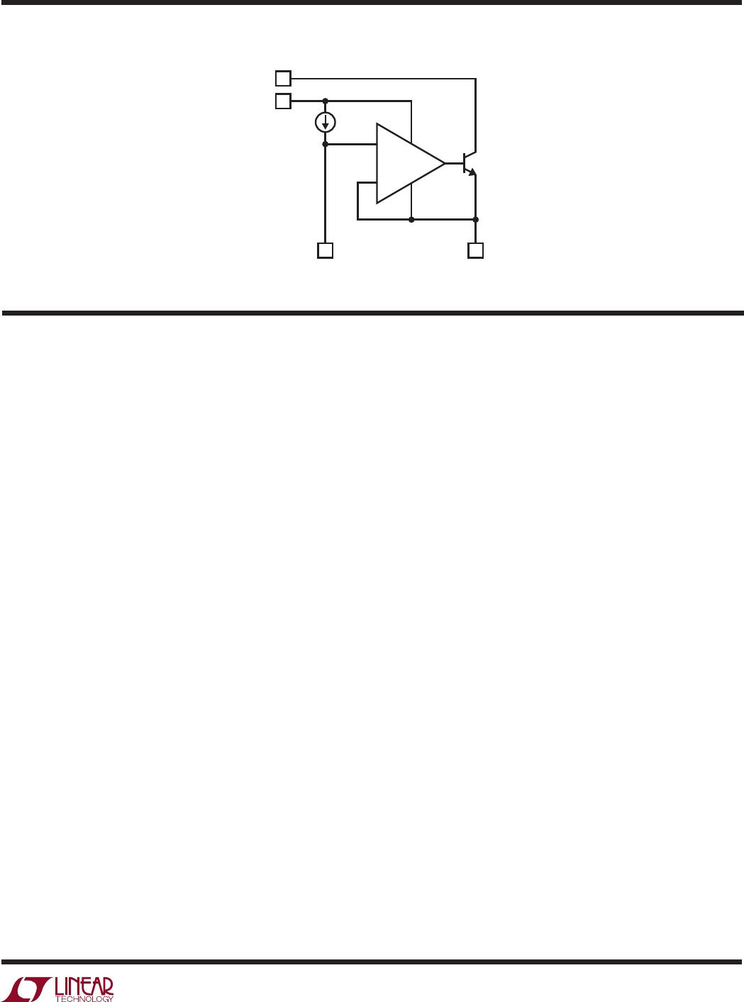
A precision “0” TC 10µA internal current source is con-
nected to the noninverting input of a power operational
amplifier. The power operational amplifier provides a low
impedance buffered output to the voltage on the noninvert-
ing input. A single resistor from the noninverting input to
ground sets the output voltage and if this resistor is set
to zero, zero output results. As can be seen, any output
voltage can be obtained from zero up to the maximum
defined by the input power supply.
What is not so obvious from this architecture are the ben-
efits of using a true internal current source as the reference
as opposed to a bootstrapped reference in older regulators.
A true current source allows the regulator to have gain
and frequency response independent of the impedance on
the positive input. Older adjustable regulators, such as the
LT1086 have a change in loop gain with output voltage
as well as bandwidth changes when the adjustment pin
is bypassed to ground. For the LT3080, the loop gain is
unchanged by changing the output voltage or bypassing.
Output regulation is not fixed at a percentage of the output
voltage but is a fixed fraction of millivolts. Use of a true
current source allows all the gain in the buffer amplifier
to provide regulation and none of that gain is needed to
amplify up the reference to a higher output voltage.
The LT3080 has the collector of the output transistor
connected to a separate pin from the control input. Since
the dropout on the collector (IN pin) is only 350mV, two
supplies can be used to power the LT3080 to reduce dis-
sipation: a higher voltage supply for the control circuitry
and a lower voltage supply for the collector. This increases
efficiency and reduces dissipation. To further spread the
heat, a resistor can be inserted in series with the collector
to move some of the heat out of the IC and spread it on
the PC board.
The LT3080 can be operated in two modes. Three-terminal
mode has the control pin connected to the power input pin
which gives a limitation of 1.35V dropout. Alternatively,
the “control” pin can be tied to a higher voltage and the
power IN pin to a lower voltage giving 350mV dropout
on the IN pin and minimizing the power dissipation. This
allows for a 1.1A supply regulating from 2.5V
IN
to 1.8V
OUT
or 1.8V
IN
to 1.2V
OUT
with low dissipation.
+
V
CONTROL
IN
10µA
3080 BD
OUTSET
block DiagraM
applicaTions inForMaTion

LT3080EDD#PBF

Mfr. #:
Manufacturer:
Analog Devices / Linear Technology
Description:
LDO Voltage Regulators Adj 1.1A 1x Res L Drop Reg
Lifecycle:
New from this manufacturer.
Delivery:
DHL FedEx Ups TNT EMS
Payment:
T/T Paypal Visa MoneyGram Western Union