Precision Micropower, Low Noise CMOS,
Rail-to-Rail Input/Output Operational Amplifiers
AD8603/AD8607/AD8609
Rev. C
Information furnished by Analog Devices is believed to be accurate and reliable. However, no
responsibility is assumed by Analog Devices for its use, nor for any infringements of patents or other
rights of third parties that may result from its use. Specifications subject to change without notice. No
license is granted by implication or otherwise under any patent or patent rights of Analog Devices.
Trademarks and registered trademarks are the property of their respective owners.
One Technology Way, P.O. Box 9106, Norwood, MA 02062-9106, U.S.A.
Tel: 781.329.4700 www.analog.com
Fax: 781.461.3113 ©2003–2008 Analog Devices, Inc. All rights reserved.
FEATURES
Low offset voltage: 50 μV maximum
Low input bias current: 1 pA maximum
Single-supply operation: 1.8 V to 5 V
Low noise: 22 nV/√Hz
Micropower: 50 μA maximum
Low distortion
No phase reversal
Unity gain stable
APPLICATIONS
Battery-powered instrumentation
Multipole filters
Sensors
Low power ASIC input or output amplifiers
GENERAL DESCRIPTION
The AD8603/AD8607/AD8609 are single/dual/quad micro-
power rail-to-rail input and output amplifiers, respectively, that
feature very low offset voltage as well as low input voltage and
current noise.
These amplifiers use a patented trimming technique that achieves
superior precision without laser trimming. The parts are fully
specified to operate from 1.8 V to 5.0 V single supply or from
±0.9 V to ±2.5 V dual supply. The combination of low offsets, low
noise, very low input bias currents, and low power consumption
makes the AD8603/AD8607/AD8609 especially useful in portable
and loop-powered instrumentation.
The ability to swing rail to rail at both the input and output
enables designers to buffer CMOS ADCs, DACs, ASICs, and
other wide output swing devices in low power, single-supply
systems.
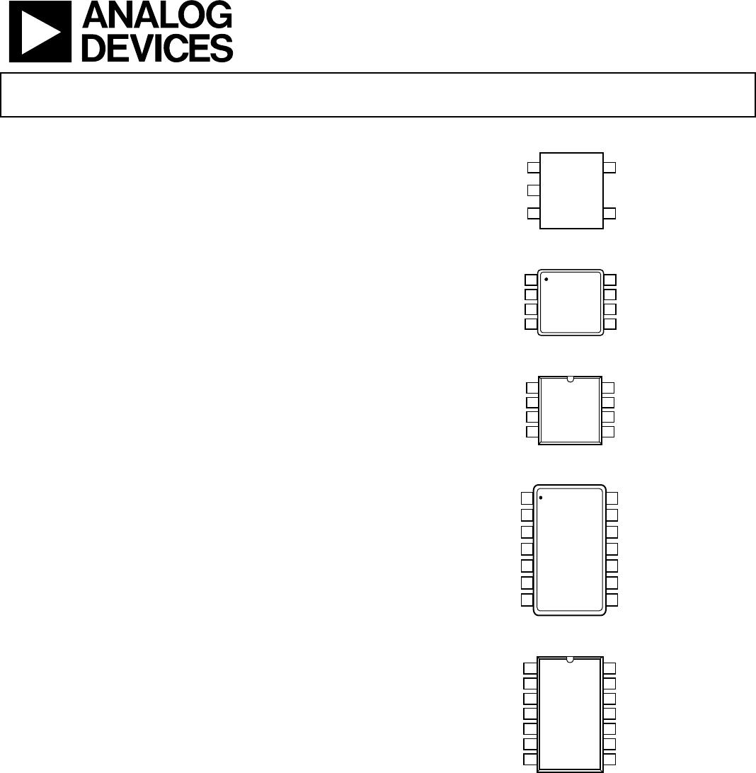
The AD8603 is available in a tiny 5-lead TSOT package. The
AD8607 is available in 8-lead MSOP and 8-lead SOIC packages.
The AD8609 is available in 14-lead TSSOP and 14-lead SOIC
packages.
PIN CONFIGURATIONS
04356-001
OUT
1
V–
2
+IN
3
V+
5
–IN
4
AD8603
TOP VIEW
(Not to Scale)
Figure 1. 5-Lead TSOT (UJ Suffix)
04356-002
OUT A
1
–IN A
2
+IN A
3
V–
4
V+
8
OUT B
7
–IN B
6
+IN B
5
AD8607
TOP VIEW
(Not to Scale)
Figure 2. 8-Lead MSOP (RM Suffix)
04356-003
OUT A
1
–IN A
2
+IN A
3
V–
4
V+
8
OUT B
7
–IN B
6
+IN B
5
AD8607
TOP VIEW
(Not to Scale)
Figure 3. 8-Lead SOIC (R Suffix)
04356-004
1
2
3
4
5
6
7
AD8609
–IN A
+IN A
V+
OUT B
–IN B
+IN B
OUT A
14
13
12
11
10
9
8
–IN D
+IN D
V–
OUT C
–IN C
+IN C
OUT D
TOP VIEW
(Not to Scale)
Figure 4. 14-Lead TSSOP (RU Suffix)
OUT A
1
–IN A
2
+IN A
3
V+
4
OUT D
14
–IN D
13
+IN D
12
V–
11
+IN B
5
+IN C
10
–IN B
6
–IN C
9
OUT B
7
OUT C
8
AD8609
TOP VIEW
(Not to Scale)
0
4356-005
Figure 5. 14-Lead SOIC (R Suffix)
AD8603/AD8607/AD8609
Rev. C | Page 2 of 16
TABLE OF CONTENTS
Features .............................................................................................. 1
Applications ....................................................................................... 1
General Description ......................................................................... 1
Pin Configurations ........................................................................... 1
Revision History ............................................................................... 2
Specifications ..................................................................................... 3
Electrical Characteristics ............................................................. 3
Absolute Maximum Ratings ............................................................ 5
ESD Caution .................................................................................. 5
Typical Performance Characteristics ............................................. 6
Applications ..................................................................................... 12
No Phase Reversal ...................................................................... 12
Input Overvoltage Protection ................................................... 12
Driving Capacitive Loads .......................................................... 12
Proximity Sensors ....................................................................... 13
Composite Amplifiers ................................................................ 13
Battery-Powered Applications .................................................. 13
Photodiodes ................................................................................ 13
Outline Dimensions ....................................................................... 14
Ordering Guide .......................................................................... 16
REVISION HISTORY
6/08—Rev. B to Rev. C
Changes to Table 1 ............................................................................ 3
Changes to Table 2 ............................................................................ 4
Changes to Figure 15 ........................................................................ 7
Changes to Figure 33 ...................................................................... 10
Changes to Figure 45 and Figure 47 ............................................. 13
Updated Outline Dimensions ....................................................... 14
Changes to Ordering Guide .......................................................... 16
6/05—Rev. A to Rev. B
Updated Figure 49 .......................................................................... 15
Changes to Ordering Guide .......................................................... 17
10/03—Rev. 0 to Rev. A
Added AD8607 and AD8609 Parts .................................. Universal
Changes to Specifications ................................................................ 3
Changes to Figure 35 ...................................................................... 10
Added Figure 41 .............................................................................. 11
8/03—Revision 0: Initial Version
AD8603/AD8607/AD8609
Rev. C | Page 3 of 16
SPECIFICATIONS
ELECTRICAL CHARACTERISTICS
V
S
= 5 V, V
CM
= V
S
/2, T
A
= 25°C, unless otherwise noted.
Table 1.
Parameter Symbol Conditions Min Typ Max Unit
INPUT CHARACTERISTICS
Offset Voltage V
OS
V
S
= 3.3 V @ V
CM
= 0.5 V and 2.8 V 12 50 μV
−0.3 V < V
CM
< +5.2 V 40 300 μV
−40°C < T
A
< +125°C, −0.3 V < V
CM
< +5.2 V 700 μV
Offset Voltage Drift ∆V
OS
/∆T −40°C < T
A
< +125°C 1 4.5 μV/°C
Input Bias Current I
B
0.2 1 pA
−40°C < T
A
< +85°C 50 pA
−40°C < T
A
< +125°C 500 pA
Input Offset Current I
OS
0.1 0.5 pA
−40°C < T
A
< +85°C 50 pA
−40°C < T
A
< +125°C 250 pA
Input Voltage Range IVR −0.3 +5.2 V
Common-Mode Rejection Ratio CMRR 0 V < V
CM
< 5 V 85 100 dB
−40°C < T
A
< +125°C 80 dB
Large Signal Voltage Gain A
VO
R
L
= 10 kΩ, 0.5 V < V
O
< 4.5 V
AD8603 400 1000 V/mV
AD8607/AD8609 250 450 V/mV
Input Capacitance C
DIFF
1.9 pF
C
CM
2.5 pF
OUTPUT CHARACTERISTICS
Output Voltage High V
OH
I
L
= 1 mA 4.95 4.97 V
−40°C to +125°C 4.9 V
I
L
= 10 mA 4.65 4.97 V
−40°C to +125°C 4.50 V
Output Voltage Low V
OL
I
L
= 1 mA 16 30 mV
−40°C to +125°C 50 mV
I
L
= 10 mA 160 250 mV
−40°C to +125°C 330 mV
Short-Circuit Current I
SC
±70 mA
Closed-Loop Output Impedance Z
OUT
f = 10 kHz, A
V
= 1 36 Ω
POWER SUPPLY
Power Supply Rejection Ratio PSRR 1.8 V < V
S
< 5 V 80 100 dB
Supply Current per Amplifier I
SY
V
O
= 0 V 40 50 μA
−40°C <T
A
< +125°C 60 μA
DYNAMIC PERFORMANCE
Slew Rate SR R
L
= 10 kΩ 0.1 V/μs
Settling Time 0.1% t
S
G = ±1, 2 V step 23 μs
Gain Bandwidth Product GBP R
L
= 100 kΩ 400 kHz
R
L
= 10 kΩ 316 kHz
Phase Margin Ø
O
R
L
= 10 kΩ, R
L
= 100 kΩ 70 Degrees
NOISE PERFORMANCE
Peak-to-Peak Noise e
n p-p
0.1 Hz to 10 Hz 2.3 3.5 μV
Voltage Noise Density e
n
f = 1 kHz 25 nV/√Hz
f = 10 kHz 22 nV/√Hz
Current Noise Density i
n
f = 1 kHz 0.05 pA/√Hz
Channel Separation C
S
f = 10 kHz −115 dB
f = 100 kHz −110 dB

AD8603AUJZ-REEL

Mfr. #:
Manufacturer:
Analog Devices Inc.
Description:
Precision Amplifiers MicroPwr RRIO Low Noise Prec SGL CMOS
Lifecycle:
New from this manufacturer.
Delivery:
DHL FedEx Ups TNT EMS
Payment:
T/T Paypal Visa MoneyGram Western Union