AD8603/AD8607/AD8609
Rev. C | Page 12 of 16
APPLICATIONS
NO PHASE REVERSAL
The AD8603/AD8607/AD8609 do not exhibit phase inversion
even when the input voltage exceeds the maximum input
common-mode voltage. Phase reversal can cause permanent
damage to the amplifier, resulting in system lockups. The
AD8603/AD8607/AD8609 can handle voltages of up to 1 V
over the supply.
VOLTAGE (1V/DIV)
TIME (4µs/DIV)
V
S
= ±2.5V
V
IN
= 6V p-p
A
V
= 1
R
L
= 10kΩ
V
IN
V
OUT
04356-041
Figure 41. No Phase Response
INPUT OVERVOLTAGE PROTECTION
If a voltage 1 V higher than the supplies is applied at either
input, the use of a limiting series resistor is recommended. If
both inputs are used, each one should be protected with a
series resistor.
To ensure good protection, the current should be limited to a
maximum of 5 mA. The value of the limiting resistor can be
determined from the following equation:
(V
IN
− V
S
)/(R
S
+ 200 Ω) ≤ 5 mA
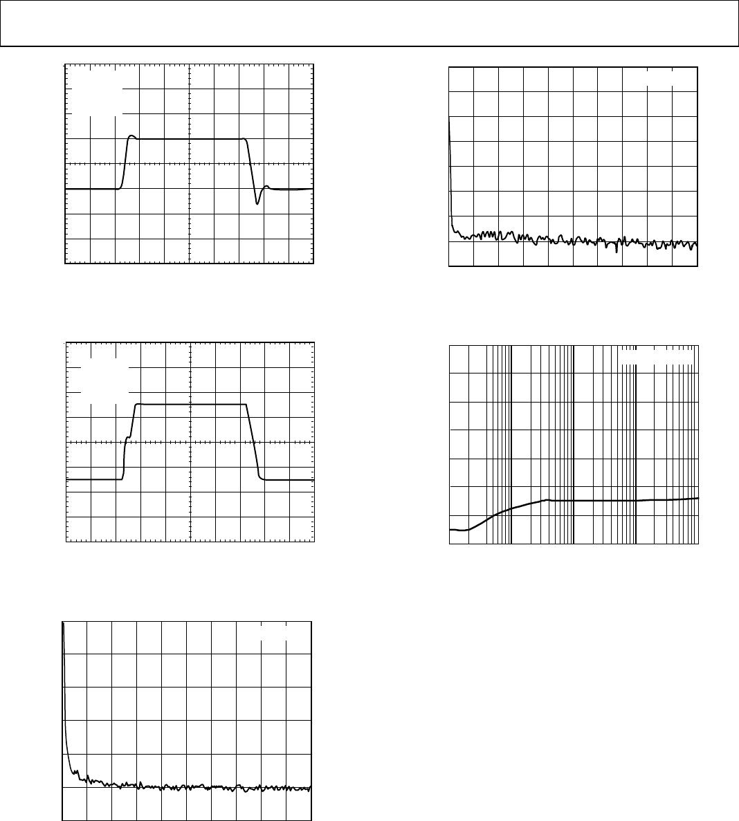
DRIVING CAPACITIVE LOADS
The AD8603/AD8607/AD8609 are capable of driving large
capacitive loads without oscillating. Figure 42 shows the output
of the AD8603/AD8607/AD8609 in response to a 100 mV input
signal, with a 2 nF capacitive load.
Although it is configured in positive unity gain (the worst case),
the AD8603 shows less than 20% overshoot. Simple additional
circuitry can eliminate ringing and overshoot.
One technique is the snubber network, which consists of a
series RC and a resistive load (see Figure 43). With the snubber
in place, the AD8603/AD8607/AD8609 are capable of driving
capacitive loads of 2 nF with no ringing and less than 3%
overshoot.
The use of the snubber circuit is usually recommended for unity
gain configurations. Higher gain configurations help improve
the stability of the circuit. Figure 44 shows the same output
response with the snubber in place.
V
S
= ±0.9V
V
IN
= 100mV
C
L
= 2nF
R
L
= 10kΩ
4356-042
Figure 42. Output Response to a 2 nF Capacitive Load, Without Snubber
04356-043
C
S
47pF
V
CC
V
EE
R
S
150Ω
200mV
C
L
V+
V–
–
+
Figure 43. Snubber Network
V
SY
= ±0.9V
V
IN
= 100mV
C
L
= 2nF
R
L
= 10kΩ
R
S
= 150Ω
C
S
= 470pF
04356-044
Figure 44. Output Response to a 2 nF Capacitive Load with Snubber
Optimum values for R
S
and C
S
are determined empirically;
Table 5 lists a few starting values.
Table 5. Optimum Values for the Snubber Network
C
L
(pF) R
S
(Ω)
C
S
(pF)
100 to ~500 500 680
1500 100 330
1600 to ~2000 400 100