ADuM3400W/ADuM3401W/ADuM3402W Data Sheet
The pulses at the transformer output have an amplitude greater
than 1.0 V. The decoder has a sensing threshold at about 0.5 V, thus
establishing a 0.5 V margin in which induced voltages can be
tolerated. The voltage induced across the receiving coil is given by
V = (−dβ/dt)∑∏r
n
2
; N = 1, 2, … , N
where:
β is magnetic flux density (gauss).
N is the number of turns in the receiving coil.
r
n
is the radius of the n
th
turn in the receiving coil (cm).
Given the geometry of the receiving coil in the ADuM3400W/
ADuM3401W/ADuM3402W and an imposed requirement that
the induced voltage be at most 50% of the 0.5 V margin at the
decoder, a maximum allowable magnetic field is calculated as
shown in Figure 19.
MAGNETIC FIELD FREQUENCY (Hz)
100
MAXIMUM ALLOWABLE MAGNETIC FLUX
DENSITY (kgauss)
0.001
1M
10
0.01
1k
10k 10M
0.1
1
100M100k
11000-019
Figure 19. Maximum Allowable External Magnetic Flux Density
For example, at a magnetic field frequency of 1 MHz, the
maximum allowable magnetic field of 0.2 kgauss induces a
voltage of 0.25 V at the receiving coil, which is about 50% of the
sensing threshold and does not cause a faulty output transition.
Similarly, if such an event were to occur during a transmitted
pulse (and was of the worst-case polarity), it would reduce the
received pulse from >1.0 V to 0.75 Vstill well above the 0.5 V
sensing threshold of the decoder.
The preceding magnetic flux density values correspond to
specific current magnitudes at given distances from the
ADuM3400W/ADuM3401W/ADuM3402W transformers.
Figure 20 expresses these allowable current magnitudes as a
function of frequency for selected distances. As shown, the
ADuM3400W/ADuM3401W/ADuM3402W is extremely
immune and can be affected only by extremely large currents
operated at high frequency very close to the component. For
the 1 MHz example noted, one would have to place a 0.5 kA
current 5 mm away from the ADuM3400W/ADuM3401W/
ADuM3402W to affect the operation of the component.
MAGNETIC FIELD FREQUENCY (Hz)
MAXIMUM ALLOWABLE CURRENT (kA)
1000
100
10
1
0.1
0.01
1k 10k 100M100k 1M 10M
DISTANCE = 5mm
DISTANCE = 1m
DISTANCE = 100mm
11000-020
Figure 20. Maximum Allowable Current for Various Current-to-
ADuM3400W/ADuM3401W/ADuM3402W Spacings
Note that at combinations of strong magnetic field and high
frequency, any loops formed by printed circuit board traces
could induce error voltages sufficiently large enough to trigger
the thresholds of succeeding circuitry. Care should be taken in
the layout of such traces to avoid this possibility.
POWER CONSUMPTION
The supply current at a given channel of the ADuM3400W/
ADuM3401W/ADuM3402W isolator is a function of the supply
voltage, the channel’s data rate, and the channels output load.
For each input channel, the supply current is given by
I
DDI
= I
DDI (Q)
f ≤ 0.5 f
r
I
DDI
= I
DDI (D)
× (2f f
r
) + I
DDI (Q)
f > 0.5 f
r
For each output channel, the supply current is given by
I
DDO
= I
DDO (Q)
f ≤ 0.5 f
r
I
DDO
= (I
DDO (D)
+ (0.5 × 10
−3
) × C
L
× V
DDO
) × (2f − f
r
) + I
DDO (Q)
f > 0.5 f
r
where:
I
DDI (D)
, I
DDO (D)
are the input and output dynamic supply currents
per channel (mA/Mbps).
C
L
is the output load capacitance (pF).
V
DDO
is the output supply voltage (V).
f is the input logic signal frequency (MHz); it is half of the input
data rate expressed in units of Mbps.
f
r
is the input stage refresh rate (Mbps).
I
DDI (Q)
, I
DDO (Q)
are the specified input and output quiescent
supply currents (mA).
Rev. B | Page 16 of 20
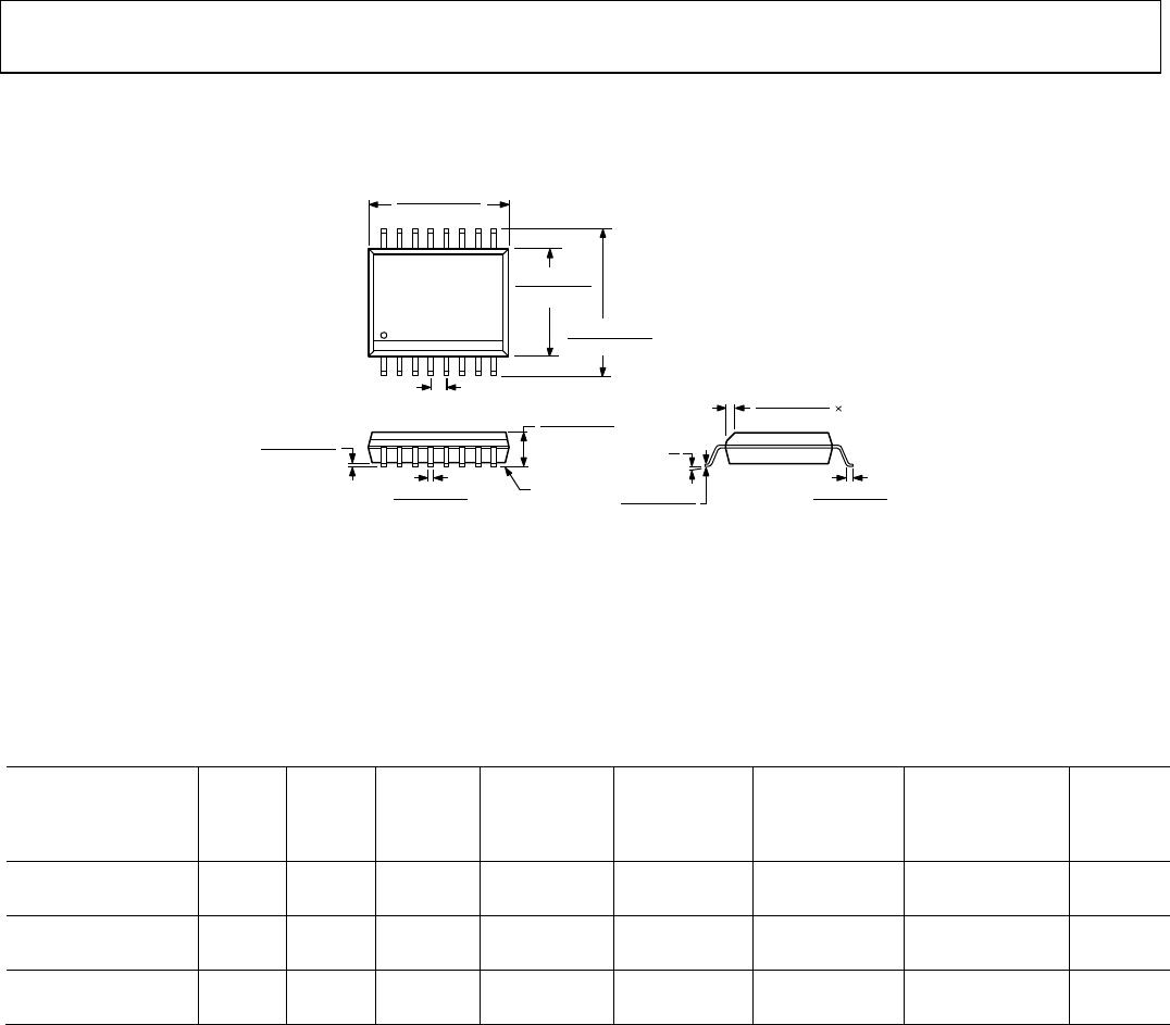
Data Sheet ADuM3400W/ADuM3401W/ADuM3402W
Rev. B | Page 17 of 20
To calculate the total I
DD1
and I
DD2
supply current, the supply
currents for each input and output channel corresponding to
V
DD1
and V
DD2
are calculated and totaled. Figure 8 provides the
per-channel input supply current as a function of the data rate.
Figure 9 and Figure 10 provide the per-channel supply output
current as a function of the data rate for an unloaded output
condition and for a 15 pF output condition, respectively. Figure 11
through Figure 15 provide the total V
DD1
and V
DD2
supply
current as a function of the data rate for ADuM3400W/
ADuM3401W/ADuM3402W channel configurations.
INSULATION LIFETIME
All insulation structures eventually break down when subjected
to voltage stress over a sufficiently long period. The rate of
insulation degradation is dependent on the characteristics of
the voltage waveform applied across the insulation. In addition
to the testing performed by the regulatory agencies, Analog
Devices carries out an extensive set of evaluations to determine
the lifetime of the insulation structure within the ADuM3400W/
ADuM3401W/ADuM3402W.
Analog Devices performs accelerated life testing using voltage
levels higher than the rated continuous working voltage.
Acceleration factors for several operating conditions are
determined. These factors allow calculation of the time to
failure at the actual working voltage. The values shown in
Figure 21 summarize the peak voltage for 50 years of service life
for a bipolar ac operating condition, and the maximum
CSA/VDE approved working voltages. In many cases, the
approved working voltage is higher than the 50-year service life
voltage. Operation at these high working voltages can lead to
shortened insulation life in some cases.
The insulation lifetime of the ADuM3400W/ADuM3401W/
ADuM3402W depends on the voltage waveform type imposed
across the isolation barrier. The iCoupler insulation structure
degrades at different rates depending on whether the waveform
is bipolar ac, unipolar ac, or dc. Figure 21, Figure 22, and
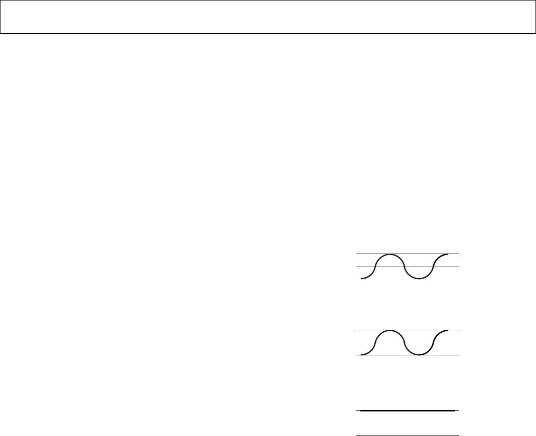
Figure 23 illustrate these different isolation voltage waveforms.
Bipolar ac voltage is the most stringent environment. The goal
of a 50-year operating lifetime under the ac bipolar condition
determines the recommended maximum working voltage of
Analog Devices.
In the case of unipolar ac or dc voltage, the stress on the
insulation is significantly lower, which allows operation at
higher working voltages while still achieving a 50-year service
life. The working voltages listed in Table 19 can be applied while
maintaining the 50-year minimum lifetime provided the voltage
conforms to either the unipolar ac or dc voltage cases. Any cross
insulation voltage waveform that does not conform to Figure 22
or Figure 23 should be treated as a bipolar ac waveform and its
peak voltage should be limited to the 50-year lifetime voltage
value listed in Table 19.
Note that the voltage presented in Figure 22 is shown as sinusoi-
dal for illustration purposes only. It is meant to represent any
voltage waveform varying between 0 V and some limiting value.
The limiting value can be positive or negative, but the voltage
cannot cross 0 V.
0V
RATED PEAK VOLTAGE
11000-021
Figure 21. Bipolar AC Waveform
0V
RATED PEAK VOLTAGE
11000-022
Figure 22. Unipolar AC Waveform
0V
RATED PEAK VOLTAGE
11000-023
Figure 23. DC Waveform
ADuM3400W/ADuM3401W/ADuM3402W Data Sheet
Rev. B | Page 18 of 20
OUTLINE DIMENSIONS
CONTROLLING DIMENSIONS ARE IN MILLIMETERS; INCH DIMENSIONS
(IN PARENTHESES) ARE ROUNDED-OFF MILLIMETER EQUIVALENTS FOR
REFERENCE ONLY AND ARE NOT APPROPRIATE FOR USE IN DESIGN.
COMPLIANT TO JEDEC STANDARDS MS-013-AA
10.50 (0.4134)
10.10 (0.3976)
0.30 (0.0118)
0.10 (0.0039)
2.65 (0.1043)
2.35 (0.0925)
10.65 (0.4193)
10.00 (0.3937)
7.60 (0.2992)
7.40 (0.2913)
0
.
7
5
(
0
.
0
2
9
5
)
0
.
2
5
(
0
.
0
0
9
8
)
45°
1.27 (0.0500)
0.40 (0.0157)
C
OPLANARITY
0.10
0.33 (0.0130)
0.20 (0.0079)
0.51 (0.0201)
0.31 (0.0122)
SEATING
PLANE
16
9
8
1
1.27 (0.0500)
BSC
03-27-2007-B
Figure 24. 16-Lead Standard Small Outline Package [SOIC_W]
Wide Body (RW-16)
Dimensions shown in millimeters and (inches)
ORDERING GUIDE
Model
1, 2, 3
Number
of
Inputs,
V
DD1
Side
Number
of
Inputs,
V
DD2
Side
Maximum
Data Rate
(Mbps)
Maximum
Propagation
Delay, 5 V (ns)
Maximum
Pulse Width
Distortion (ns)
Temperature
Range
Package
Description
Package
Option
ADuM3400WARWZ 4 0 1 100 40 −4C to +12C 16-Lead SOIC_W RW-16
ADuM3400WBRWZ 4 0 10 36 3.5 −4C to +12C 16-Lead SOIC_W RW-16
ADuM3401WARWZ 3 1 1 100 40 −4C to +12C 16-Lead SOIC_W RW-16
ADuM3401WBRWZ 3 1 10 36 3.5 −4C to +12C 16-Lead SOIC_W RW-16
ADuM3402WARWZ 2 2 1 100 40 −4C to +12C 16-Lead SOIC_W RW-16
ADuM3402WBRWZ 2 2 10 36 3.5 −4C to +12C 16-Lead SOIC_W RW-16
1
Z = RoHS Compliant Part.
2
Tape and reel are available. The addition of an -RL suffix designates a 13” (1,000 units) tape-and-reel option.
3
W = Qualified for Automotive Applications.
AUTOMOTIVE PRODUCTS
The ADuM3400W/ADuM3401W/ADuM3402W models are available with controlled manufacturing to support the quality and
reliability requirements of automotive applications. Note that these automotive models may have specifications that differ from the
commercial models; therefore, designers should review the Specifications section of this data sheet carefully. Only the automotive grade
products shown are available for use in automotive applications. Contact your local Analog Devices account representative for specific
product ordering information and to obtain the specific Automotive Reliability reports for these models.

ADUM3401WBRWZ-RL

Mfr. #:
Manufacturer:
Analog Devices Inc.
Description:
Digital Isolators 3-5.5V DC 10Mbit/s 4Chnl Dgtl 2Txr2 xr
Lifecycle:
New from this manufacturer.
Delivery:
DHL FedEx Ups TNT EMS
Payment:
T/T Paypal Visa MoneyGram Western Union