Data Sheet ADuM3400W/ADuM3401W/ADuM3402W
PACKAGE CHARACTERISTICS
Table 13.
Parameter Symbol Min Typ Max Unit Test Conditions
Resistance (Input-to-Output)
1
R
I-O
10
12
Capacitance (Input-to-Output)
1
C
I-O
2.2 pF f = 1 MHz
Input Capacitance
2
C
I
4.0 pF
IC Junction-to-Case Thermal Resistance, Side 1 θ
JCI
33 °C/W Thermocouple located at
center of package underside
IC Junction-to-Case Thermal Resistance, Side 2 θ
JCO
28 °C/W
1
Device considered a 2-terminal device; Pin 1 to Pin 8 are shorted together and Pin 9 to Pin 16 are shorted together.
2
Input capacitance is from any input data pin to ground.
REGULATORY INFORMATION
The ADuM3400W/ADuM3401W/ADuM3402W is approved by the organizations listed in Table 14. Refer to Table 19 and the Insulation
Lifetime section for details regarding recommended maximum working voltages for specific crossisolation waveforms and insulation
levels.
Table 14.
UL CSA VDE
Recognized under
1577 component recognition program
1
Approved under
CSA Component Acceptance Notice #5A
Certified according to DIN V VDE V 0884-10
(VDE V 0884-10): 2006-12
2
Single protection,
2500 V rms isolation voltage
Basic insulation per CSA 60950-1-03 and
IEC 60950-1, 800 V rms (1131 V peak)
maximum working voltage
Reinforced insulation, 560 V peak
Reinforced insulation per CSA 60950-1-03
and IEC 60950-1, 400 V rms (566 V peak)
maximum working voltage
File E214100 File 205078 File 2471900-4880-0001
1
In accordance with UL 1577, each ADuM3400W/ADuM3401W/ADuM3402W is proof tested by applying an insulation test voltage ≥3000 V rms for 1 sec (current
leakage detection limit = 5 µA).
2
In accordance with DIN V VDE V 0884-10, each ADuM3400W/ADuM3401W/ADuM3402W is proof tested by applying an insulation test voltage ≥1050 V peak for 1 sec
(partial discharge detection limit = 5 pC). The * marking branded on the component designates DIN V VDE V 0884-10
approval.
INSULATION AND SAFETY-RELATED SPECIFICATIONS
Table 15.
Parameter Symbol Value Unit Conditions
Rated Dielectric Insulation Voltage 2500 V rms 1-minute duration
Minimum External Air Gap (Clearance) L(I01) 7.7 min mm Measured from input terminals to output terminals,
shortest distance through air
Minimum External Tracking (Creepage) L(I02) 8.1 min mm Measured from input terminals to output terminals,
shortest distance path along body
Minimum Internal Gap (Internal Clearance) 0.017 min mm Insulation distance through insulation
Tracking Resistance (Comparative Tracking Index) CTI >175 V DIN IEC 112/VDE 0303 Part 1
Isolation Group IIIa Material Group (DIN VDE 0110, 1/89, Table 1)
Rev. B | Page 7 of 20
ADuM3400W/ADuM3401W/ADuM3402W Data Sheet
DIN V VDE V 0884-10 (VDE V 0884-10) INSULATION CHARACTERISTICS
These isolators are suitable for reinforced electrical isolation only within the safety limit data. Maintenance of the safety data is ensured by
protective circuits. The * marking on packages denotes DIN V VDE V 0884-10 approval.
Table 16.
Description Conditions Symbol Characteristic Unit
Installation Classification per DIN VDE 0110
For Rated Mains Voltage 150 V rms I to IV
For Rated Mains Voltage 300 V rms I to III
For Rated Mains Voltage 400 V rms I to II
Climatic Classification 40/105/21
Pollution Degree per DIN VDE 0110, Table 1 2
Maximum Working Insulation Voltage V
IORM
560 V peak
Input-to-Output Test Voltage, Method B1 V
IORM
× 1.875 = V
PR
, 100% production test,
t
m
= 1 sec, partial discharge < 5 pC
V
PR
1050 V peak
Input-to-Output Test Voltage, Method A V
IORM
× 1.6 = V
PR
, t
m
= 60 sec,
partial discharge < 5 pC
V
PR
After Environmental Tests Subgroup 1 896 V peak
After Input and/or Safety Test Subgroup 2 and Subgroup 3 V
IORM
× 1.2 = V
PR
, t
m
= 60 sec,
partial discharge < 5 pC
672 V peak
Highest Allowable Overvoltage Transient overvoltage, t
TR
= 10 seconds V
TR
4000 V peak
Safety-Limiting Values Maximum value allowed in the
event of a failure (see Figure 4)
Case Temperature T
S
150 °C
Side 1 Current I
S1
265 mA
Side 2 Current I
S2
335 mA
Insulation Resistance at T
S
V
IO
= 500 V R
S
>10
9
0
0.5
1.0
1.5
2.0
2.5
3.0
0 50 100 150 200
SAFE LIMITING POWER (W)
AMBIENT TEMPERATUREC)
11000-004
Figure 4. Thermal Derating Curve, Dependence of Safety-Limiting Values
with Ambient Temperature per DIN V VDE V 0884-10
RECOMMENDED OPERATING CONDITIONS
Table 17.
Parameter Rating
Operating Temperature Range (T
A
) −40°C to +125°C
Supply Voltages (V
DD1
, V
DD2
)
1
3.135 V to 5.5 V
Input Signal Rise and Fall Times 1.0 ms
1
All voltages are relative to their respective ground. See the DC Correctness
and Magnetic Field Immunity section for information on immunity to external
magnetic fields.
Rev. B | Page 8 of 20
Data Sheet ADuM3400W/ADuM3401W/ADuM3402W
ABSOLUTE MAXIMUM RATINGS
Ambient temperature = 25°C, unless otherwise noted.
Table 18.
Parameter Rating
Storage Temperature Range (T
ST
) −65°C to +150°C
Ambient Operating Temperature Range (T
A
) −40°C to +125°C
Supply Voltages (V
DD1
, V
DD2
)
1
−0.5 V to +7.0 V
Input Voltage (V
IA
, V
IB
, V
IC
, V
ID
, V
E1
,V
E2
)
1, 2
−0.5 V to V
DD1
+ 0.5 V
Output Voltage (V
OA
, V
OB
,V
OC
, V
OD
)
1, 2
−0.5 V to V
DDO
+ 0.5 V
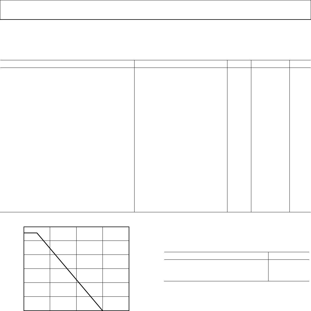
Average Output Current per Pin
3
Side 1 (I
O1
) −18 mA to +18 mA
Side 2 (I
O2
) −22 mA to + 22 mA
Common-Mode Transients (CM
H
, CM
L
)
4
−100 kV/µs to
+100 kV/µs
1
All voltages are relative to their respective ground.
2
V
DDI
and V
DDO
refer to the supply voltages on the input and output sides of a
given channel, respectively. See the PC Board Layout section.
3
See Figure 4 for maximum rated current values for various temperatures.
4
Refers to common-mode transients across the insulation barrier. Common-
mode transients exceeding the Absolute Maximum Ratings can cause latch-
up or permanent damage.
Stresses at or above those listed under Absolute Maximum
Ratings may cause permanent damage to the product. This is a
stress rating only; functional operation of the product at these
or any other conditions above those indicated in the operational
section of this specification is not implied. Operation beyond
the maximum operating conditions for extended periods may
affect product reliability.
ESD CAUTION
Table 19. Maximum Continuous Working Voltage
1
Parameter Max Unit Constraint
AC Voltage, Bipolar Waveform 565 V peak 50-year minimum lifetime
AC Voltage, Unipolar Waveform
Basic Insulation 1131 V peak Maximum approved working voltage per IEC 60950-1
Reinforced Insulation 560 V peak Maximum approved working voltage per IEC 60950-1 and VDE V 0884-10
DC Voltage
Basic Insulation 1131 V peak Maximum approved working voltage per IEC 60950-1
Reinforced Insulation 560 V peak Maximum approved working voltage per IEC 60950-1 and VDE V 0884-10
1
Refers to continuous voltage magnitude imposed across the isolation barrier. See the Insulation Lifetime section for more details.
Table 20. Truth Table (Positive Logic)
V
Ix
Input
1
V
Ex
Input
2
V
DDI
State
1
V
DDO
State
1
V
OX
Output
1
Notes
H H or NC Powered Powered H
L H or NC Powered Powered L
x L Powered Powered Z
x H or NC Unpowered Powered H Outputs return to the input state within 1 µs of V
DDI
power restoration.
x L Unpowered Powered Z
x
x
Powered
Unpowered
Indeterminate
Outputs return to the input state within 1 µs of V
DDO
power restoration
if V
Ex
state is H or NC. Outputs return to high impedance state within
8 ns of V
DDO
power restoration if V
Ex
state is L.
1
V
Ix
and V
Ox
refer to the input and output signals of a given channel (A, B, C, or D). V
Ex
refers to the output enable signal on the same side as the V
Ox
outputs. V
DDI
and
V
DDO
refer to the supply voltages on the input and output sides of the given channel, respectively.
2
In noisy environments, connecting V
Ex
to an external logic high or low is recommended.
Rev. B | Page 9 of 20

ADUM3401WBRWZ-RL

Mfr. #:
Manufacturer:
Analog Devices Inc.
Description:
Digital Isolators 3-5.5V DC 10Mbit/s 4Chnl Dgtl 2Txr2 xr
Lifecycle:
New from this manufacturer.
Delivery:
DHL FedEx Ups TNT EMS
Payment:
T/T Paypal Visa MoneyGram Western Union