October 2011 Doc ID 11265 Rev 5 1/14
14
USBLC6-2
Very low capacitance ESD protection
Features
2 data-line protection
Protects V
BUS
Very low capacitance: 3.5 pF max.
Very low leakage current: 150 nA max.
SOT-666 and SOT23-6L packages
RoHS compliant
Benefits
Very low capacitance between lines to GND for
optimized data integrity and speed
Low PCB space consumption: 2.9 mm
2
max for
SOT-666 and 9 mm² max for SOT23-6L
Enhanced ESD protection: IEC 61000-4-2
level 4 compliance guaranteed at device level,
hence greater immunity at system level
ESD protection of V
BUS
High reliability offered by monolithic integration
Low leakage current for longer operation of
battery powered devices
Fast response time
Consistent D+ / D- signal balance:
Very low capacitance matching tolerance
I/O to GND = 0.015 pF
Compliant with USB 2.0 requirements
Complies with the following standards:
IEC 61000-4-2 level 4:
15 kV (air discharge)
8 kV (contact discharge)
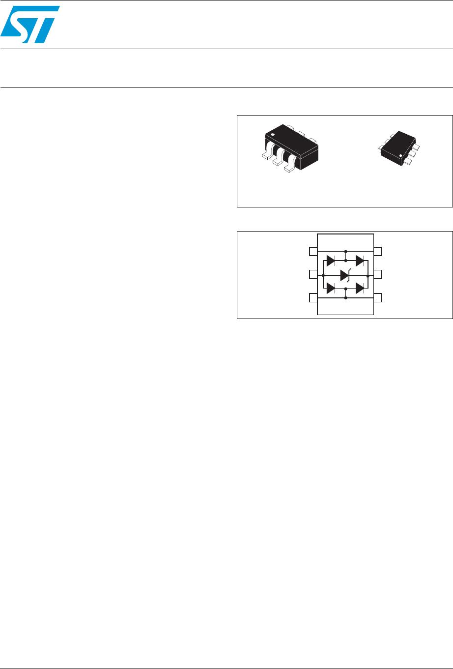
Figure 1. Functional diagram (top view)
Applications
USB 2.0 ports up to 480 Mb/s (high speed)
Compatible with USB 1.1 low and full speed
Ethernet port: 10/100 Mb/s
SIM card protection
Video line protection
Portable electronics
Description
The USBLC6-2SC6 and USBLC6-2P6 are
monolithic application specific devices dedicated
to ESD protection of high speed interfaces, such
as USB 2.0, Ethernet links and video lines.
The very low line capacitance secures a high level
of signal integrity without compromising in
protecting sensitive chips against the most
stringently characterized ESD strikes.
SOT23-6L
USBLC6-2SC6
SOT-666
USBLC6-2P6
11
6
2
5
3
4
I/O1 I/O1
GND V
BUS
I/O2 I/O2
www.st.com
Characteristics USBLC6-2
2/14 Doc ID 11265 Rev 5
1 Characteristics
Table 1. Absolute ratings
Symbol Parameter Value Unit
V
PP
Peak pulse voltage
IEC 61000-4-2 air discharge
IEC 61000-4-2 contact discharge
MIL STD883G-Method 3015-7
15
15
25
kV
T
stg
Storage temperature range -55 to +150 °C
T
j
Operating junction temperature range -40 to +125 °C
T
L
Lead solder temperature (10 seconds duration) 260 °C
Table 2. Electrical characteristics (T
amb
= 25 °C)
Symbol Parameter Test conditions
Value
Unit
Min. Typ. Max.
I
RM
Leakage current V
RM
= 5.25 V 10 150 nA
V
BR
Breakdown voltage between
V
BUS
and GND
I
R
= 1 mA 6 V
V
F
Forward voltage I
F
= 10 mA 1.1 V
V
CL
Clamping voltage
I
PP
= 1 A, 8/20 µs
Any I/O pin to GND
12 V
I
PP
= 5 A, 8/20 µs
Any I/O pin to GND
17 V
C
i/o-GND
Capacitance between I/O
and GND
V
R
= 1.65 V 2.5 3.5
pF
ΔC
i/o-GND
0.015
C
i/o-i/o
Capacitance between I/O V
R
= 1.65 V 1.2 1.7
pF
ΔC
i/o-i/o
0.04
USBLC6-2 Characteristics
Doc ID 11265 Rev 5 3/14
Figure 2. Capacitance versus voltage
(typical values)
Figure 3. Line capacitance versus frequency
(typical values)
0.0
0.5
1.0
1.5
2.0
2.5
3.0
0.0 0.5 1.0 1.5 2.0 2.5 3.0 3.5 4.0 4.5 5.0
C(pF)
F=1MHz
V =30mV
T =25°C
OSC RMS
j
C =I/O-I/O
j
C =I/O-GND
O
Data line voltage (V)
0.0
0.2
0.4
0.6
0.8
1.0
1.2
1.4
1.6
1.8
2.0
2.2
2.4
2.6
2.8
1 10 100 1000
C(pF)
V =30mV
T =25°C
OSC RMS
j
V =0V to 3.3V
LINE
F(MHz)
Figure 4. Relative variation of leakage
current versus junction
temperature (typical values)
Figure 5. Frequency response
1
10
100
25 50 75 100 125
T (°C)
j
V =5V
BUS
I[T
RM j
] / I [T
RM j
=25°C]
100.0k 1.0M 10.0M 100.0M 1.0G
-20.00
-15.00
-10.00
-5.00
0.00
S21(dB)
F(Hz)

USBLC6-2SC6

Mfr. #:
Manufacturer:
STMicroelectronics
Description:
TVS Diodes / ESD Suppressors ESD Protection Low Cap
Lifecycle:
New from this manufacturer.
Delivery:
DHL FedEx Ups TNT EMS
Payment:
T/T Paypal Visa MoneyGram Western Union

Products related to this Datasheet