Technical information USBLC6-2
4/14 Doc ID 11265 Rev 5
2 Technical information
2.1 Surge protection
The USBLC6-2 is particularly optimized to perform surge protection based on the rail to rail
topology.
The clamping voltage V
CL
can be calculated as follow:
V
CL
+ = V
TRANSIL
+ V
F
for positive surges
V
CL
- = - V
F
for negative surges
with: V
F
= V
T
+ R
d
.I
p
(V
F
forward drop voltage) / (V
T
forward drop threshold voltage)
and V
TRANSIL
= V
BR
+ R
d_TRANSIL
.I
P
Calculation example
We assume that the value of the dynamic resistance of the clamping diode is typically:
R
d
= 0.5 Ω and V
T
= 1.1 V
We assume that the value of the dynamic resistance of the transil diode is typically:
R
d_TRANSIL
= 0.5 Ω and V
BR
= 6.1 V
For an IEC 61000-4-2 surge Level 4 (Contact Discharge: V
g
= 8 kV, R
g
= 330 Ω),
V
BUS
= +5 V, and if in first approximation, we assume that:
I
p
= V
g
/ R
g
= 24 A.
So, we find:
V
CL
+ = +31.2 V
V
CL
- = -13 V
Note: The calculations do not take into account phenomena due to parasitic inductances.
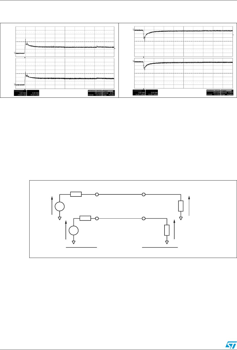
2.2 Surge protection application example
If we consider that the connections from the pin V
BUS
to V
CC
, from I/O to data line and from
GND to PCB GND plane are done by tracks of 10 mm long and 0.5 mm large, we assume
that the parasitic inductances L
VBUS
, L
I/O
and L
GND
of these tracks are about 6 nH. So when
an IEC 61000-4-2 surge occurs on data line, due to the rise time of this spike (t
r
=1ns), the
voltage V
CL
has an extra value equal to L
I/O
.dl/dt + L
GND
.dI/dt.
The dI/dt is calculated as:
dI/dt = I
p
/t
r
= 24 A/ns
The overvoltage due to the parasitic inductances is:
L
I/O
.dl/dt = L
GND
.dI/dt = 6 nH x 24 A/ns = 144 V
By taking into account the effect of these parasitic inductances due to unsuitable layout, the
clamping voltage will be:
V
CL
+ = +31.2 + 144 + 144 = 319.2 V
V
CL
- = -13.1 - 144 - 144 = -301.1 V
USBLC6-2 Technical information
Doc ID 11265 Rev 5 5/14
We can significantly reduce this phenomena with simple layout optimization. It is for this
reason that some recommendations have to be followed (see 2.3: How to ensure good ESD
protection).
Figure 6. ESD behavior: parasitic phenomena due to unsuitable layout
2.3 How to ensure good ESD protection
While the USBLC6-2 provides high immunity to ESD surge, efficient protection depends on
the layout of the board. In the same way, with the rail to rail topology, the track from data
lines to I/O pins, from V
CC
to V
BUS
pin and from GND plane to GND pin must be as short as
possible to avoid overvoltages due to parasitic phenomena (see Figure 6. and Figure 7. for
layout consideration)
V
BUS
L
I/O
L
VBUS
L
GND
L
I/O
L
GND
V pin
CC
V
CL
V
F
I/O pin
V
TRANSIL
V+V
TRANSIL F
-V
F
V
CL-
t = 1 ns
r
t
t
t = 1 ns
r
V
CL+
GND pin
Data line
Positive
Surge
Negative
Surge
ESD surge on data line
di
dt
L
I/O
+ L
GND
di
dt
di
dt
-L
I/O
- L
GND
di
dt
di
dt
V
+
=V +V + L + L
surge > 0
CL TRANSIL F I/O GND
V = -V - L - L
surge > 0
CL- F I/O GND
di
dt
di
dt
di
dt
di
dt
di
dt
Rd.IpVV
BR
TRANSIL
+=
Figure 7. ESD behavior: layout optimization Figure 8. ESD behavior: measurement
conditions
Unsuitable layout
Optimized layout
1
1
6
2
5
3
4
1
1
6
2
5
3
4
+5 V
IN OUT
TEST BOARD
ESD SURGE
USBLC6-2SC6
Technical information USBLC6-2
6/14 Doc ID 11265 Rev 5
Important:
A good precaution to take is to put the protection device as close as possible to the
disturbance source (generally the connector).
2.4 Crosstalk behavior
2.4.1 Crosstalk phenomenon
Figure 11. Crosstalk phenomenon
The crosstalk phenomenon is due to the coupling between 2 lines. The coupling factor (β12
or β21) increases when the gap across lines decreases, particularly in silicon dice. In the
above example the expected signal on load R
L2
is α
2
V
G2
, in fact the real voltage at this point
has got an extra value β
21
V
G1
. This part of the V
G1
signal represents the effect of the
crosstalk phenomenon of the line 1 on the line 2. This phenomenon has to be taken into
account when the drivers impose fast digital data or high frequency analog signals in the
disturbing line. The perturbed line will be more affected if it works with low voltage signal or
high load impedance (few kΩ).
Figure 9. ESD response to IEC 61000-4-2
(+15 kV air discharge)
Figure 10. ESD response to IEC 61000-4-2
(-15 kV air discharge)
Vin
Vout
Vin
Vout
Line 1
Line 2
V
G1
V
G2
R
G1
R
G2
DRIVERS
R
L1
R
L2
RECEIVERS
α
β
+
1
12
V
G1
V
G2
α
β
+
2
21
V
G2
V
G1

USBLC6-2SC6

Mfr. #:
Manufacturer:
STMicroelectronics
Description:
TVS Diodes / ESD Suppressors ESD Protection Low Cap
Lifecycle:
New from this manufacturer.
Delivery:
DHL FedEx Ups TNT EMS
Payment:
T/T Paypal Visa MoneyGram Western Union

Products related to this Datasheet