85104I Data Sheet
©2016 Integrated Device Technology, Inc Revision A January 20, 201613
3. Calculations and Equations.
The purpose of this section is to calculate power dissipation on the IC per HCSL output pair.
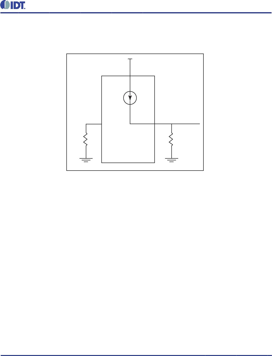
HCSL output driver circuit and termination are shown in Figure 5.
HCSL is a current steering output which sources a maximum of 17mA of current per output. To calculate worst case on-chip power
dissipation, use the following equations which assume a 50Ω load to ground.
The highest power dissipation occurs when V
DD
is HIGH.
Power = (V
DD_HIGH
– V
OUT
) * I
OUT,
since V
OUT
= I
OUT
* R
L
= (V
DD_HIGH
– I
OUT
*
R
L
) * I
OUT
= (3.63V – 17mA * 50Ω) * 17mA
Total Power Dissipation per output pair = 47.3mW
FIGURE 5. HCSL DRIVER CIRCUIT AND TERMINATION
V
DD
V
OUT
R
L
50
IC
I
OUT
= 17mA
R
REF
=
475
± 1%