85104I Data Sheet
©2016 Integrated Device Technology, Inc Revision A January 20, 20164
TABLE 4A. POWER SUPPLY DC CHARACTERISTICS, V
DD
= 3.3V±10%, TA = -40°C TO 85°C
TABLE 4B. LVCMOS / LVTTL DC CHARACTERISTICS, V
DD
= 3.3V±10%, TA = -40°C TO 85°C
TABLE 4C. DIFFERENTIAL DC CHARACTERISTICS, V
DD
= 3.3V±10%, TA = -40°C TO 85°C
ABSOLUTE MAXIMUM RATINGS
Supply Voltage, V
DD
4.6V
Inputs, V
I
-0.5V to V
DD
+ 0.5V
Outputs, I
O
-0.5V to V
DD
+ 0.5V
Package Thermal Impedance, θ
JA
91.1°C/W (0 mps)
Storage Temperature, T
STG
-65°C to 150°C
NOTE: Stresses beyond those listed under Absolute
Maximum Ratings may cause permanent damage to the
device. These ratings are stress specifi cations only. Functional
operation of product at these conditions or any conditions beyond
those listed in the DC Characteristics or AC Characteristics is not
implied. Exposure to absolute maximum rating conditions for ex-
tended periods may affect product reliability.
Symbol Parameter Test Conditions Minimum Typical Maximum Units
V
DD
Positive Supply Voltage 2.97 3.3 3.63 V
I
DD
Power Supply Current Unterminated 27 mA
Symbol Parameter Test Conditions Minimum Typical Maximum Units
V
IH
Input High Voltage 2 V
DD
+ 0.3 V
V
IL
Input Low Voltage -0.3 0.8 V
I
IH
Input
High Current
CLK1, CLK_SEL V
IN
= V
DD
= 3.63V 150 µA
CLK_EN V
IN
= V
DD
= 3.63V 5 µA
I
IL
Input
Low Current
CLK1, CLK_SEL V
IN
= 0V, V
DD
= 3.63V -5 µA
CLK_EN V
IN
= 0V, V
DD
= 3.63V -150 µA
Symbol Parameter Test Conditions Minimum Typical Maximum Units
I
IH
Input High Current CLK0/nCLK0 V
DD
= V
IN
= 3.63V 150 µA
I
IL
Input Low Current
CLK0 V
DD
= 3.63V, V
IN
= 0V -5 µA
nCLK0 V
DD
= 3.63V, V
IN
= 0V -150 µA
V
PP
Peak-to-Peak Input Voltage; NOTE 1 0.15 1.3 V
V
CMR
Common Mode Input Voltage; NOTE 1, 2 GND + 0.5 V
DD
- 0.85 V
NOTE 1: V
IL
should not be less than -0.3V.
NOTE 2: Common mode voltage is defi ned as V
IH
.
85104I Data Sheet
©2016 Integrated Device Technology, Inc Revision A January 20, 20165
TABLE 5. AC CHARACTERISTICS, V
DD
= 3.3V±10%, TA = -40°C TO 85°C
Symbol Parameter Test Conditions Minimum Typical Maximum Units
f
OUT
Output Frequency
CLK_SEL = 0 500 MHz
CLK_SEL = 1 250 MHz
t
PD
Propagation Delay; NOTE 1
CLK_SEL = 0 2.0 3.2 ns
CLK_SEL = 1 2.0 2.8 ns
tsk(o) Output Skew; NOTE 2, 4 100 ps
tsk(pp) Part-to-Part Skew; NOTE 3, 4 600 ps
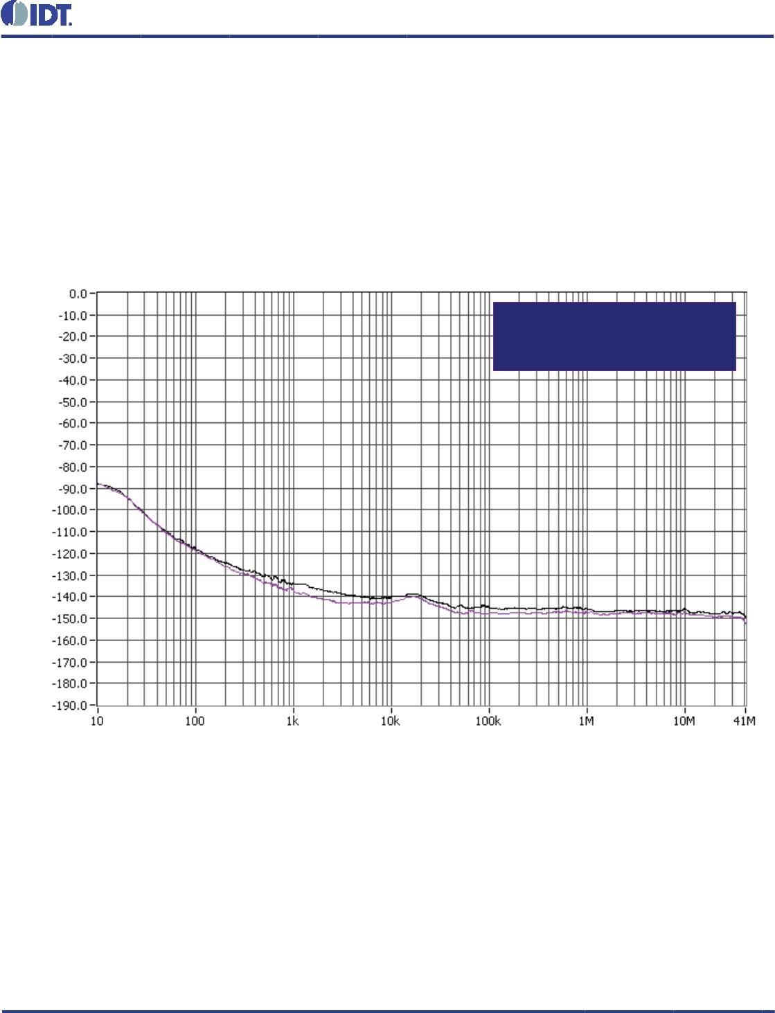
tjit
Buffer Additive Phase Jitter, RMS;
refer to Additive Phase Jitter Section
100MHz, (12kHz - 20MHz) 0.22 ps
V
MAX
Absolute Maximum Output Voltage; NOTE
5, 10
1150 mV
V
MIN
Absolute Minimum Output Voltage;
NOTE 5, 11
-300 mV
V
RB
Ringback Voltage; NOTE 6, 13 -100 100 mV
t
STABLE
Time before V
RB
is allowed; NOTE 6, 13 500 ps
V
CROSS
Absolute Crossing Voltage; NOTE 5, 8, 9 250 550 mV
DV
CROSS
Total Variation of V
CROSS
over all edges;
NOTE 5, 8, 12
140 mV
Rise/Fall Edge Rate; NOTE 6, 7
Measured between
-150mV to +150mV
0.6 5.5 V/ns
odc Output Duty Cycle; NOTE 14 45 55 %
NOTE: Electrical parameters are guaranteed over the specifi ed ambient operating temperature range, which is established when the
device is mounted in a test socket with maintained transverse airfl ow greater than 500 lfpm. The device will meet specifi cations after
thermal equilibrium has been reached under these conditions.
NOTE: All parameters measured at ƒout 250MHz unless noted otherwise.
NOTE 1: Measured from the V
DD
/2 of the input to the differential output crossing point.
NOTE 2: Defi ned as skew between outputs at the same supply voltage and with equal load conditions. Measured at the output differen-
tial cross points.
NOTE 3: Defi ned as skew between outputs on different devices operating at the same supply voltage, same temperature, and with
equal load conditions. Using the same type of inputs on each device, the outputs are measured at the differential cross points.
NOTE 4: This parameter is defi ned in accordance with JEDEC Standard 65.
NOTE 5: Measurement taken from single-ended waveform.
NOTE 6: Measurement taken from differential waveform.
NOTE 7: Measured from -150mV to +150mV on the differential waveform (derived from Qx minus nQx). The signal must be monotonic
through the measurement region for rise and fall time. The 300mV measurement window is centered on the differential zero crossing.
See Parameter Measurement Information Section.
NOTE 8: Measured at crossing point where the instantaneous voltage value of the rising edge of Qx equals the falling edge of nQx.
See Parameter Measurement Information Section.
NOTE 9: Refers to the total variation from the lowest crossing point to the highest, regardless of which edge is crossing. Refers to all
crossing points for this measurement. See Parameter Measurement Information Section.
NOTE 10: Defi ned as the maximum instantaneous voltage including overshoot. See Parameter Measurement Information Section.
NOTE 11: Defi ned as the minimum instantaneous voltage including undershoot. See Parameter Measurement Information Section.
NOTE 12: Defi ned as the total variation of all crossing voltage of Rising Qx and Falling nQx. This is the maximum allowed variance in
the V
CROSS
for any particular system. See Parameter Measurement Information Section.
NOTE: 13. T
STABLE
is the time the differential clock must maintain a minimum ±150mV differential voltage after rising/falling edges before
it is allowed to droop back into the V
RB
±100mV differential range. See Parameter Measurement Information Section.
NOTE 14: Input duty cycle must be 50%.
85104I Data Sheet
©2016 Integrated Device Technology, Inc Revision A January 20, 20166
ADDITIVE PHASE JITTER
Additive Phase Jitter,
Integration Range: 12kHz - 20MHz at
100MHz = 0.22ps (typical)
The spectral purity in a band at a specifi c offset from the fundamental
compared to the power of the fundamental is called the dBc Phase
Noise. This value is normally expressed using a Phase noise plot
and is most often the specifi ed plot in many applications. Phase
noise is defi ned as the ratio of the noise power present in a 1Hz
band at a specifi ed offset from the fundamental frequency to the
power value of the fundamental. This ratio is expressed in decibels
As with most timing specifi cations, phase noise measurements has
issues relating to the limitations of the equipment. Often the noise
oor of the equipment is higher than the noise fl oor of the device.
(dBm) or a ratio of the power in the 1Hz band to the power in the
fundamental. When the required offset is specifi ed, the phase noise
is called a dBc value, which simply means dBm at a specifi ed offset
from the fundamental. By investigating jitter in the frequency domain,
we get a better understanding of its effects on the desired application
over the entire time record of the signal. It is mathematically possible
to calculate an expected bit error rate given a phase noise plot.
This is illustrated above. The device meets the noise fl oor of what
is shown, but can actually be lower. The phase noise is dependent
on the input source and measurement equipment.
OFFSET FROM CARRIER FREQUENCY (HZ)
SSB PHASE NOISE dBc/HZ

85104AGILF

Mfr. #:
Manufacturer:
IDT
Description:
Clock Buffer DIFFERENTIAL CLOCK
Lifecycle:
New from this manufacturer.
Delivery:
DHL FedEx Ups TNT EMS
Payment:
T/T Paypal Visa MoneyGram Western Union

Products related to this Datasheet