BAP55LX All information provided in this document is subject to legal disclaimers. © NXP B.V. 2013. All rights reserved.
Product data sheet Rev. 4 — 6 August 2013 2 of 16
NXP Semiconductors
BAP55LX
Silicon PIN diode
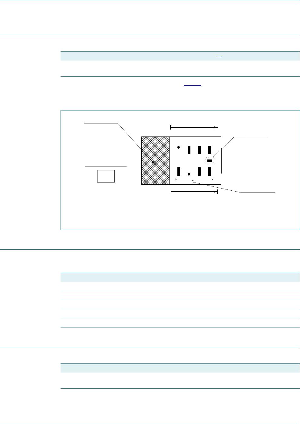
4. Marking
[1] For SOD882D binary marking code description, see Figure 1.
4.1 Binary marking code description
5. Limiting values
6. Thermal characteristics
Table 3. Marking codes
Type number Marking code
[1]
BAP55LX 1111
1101
Fig 1. SOD882D binary marking code description example
VENDOR CODE
MARKING CODE
(EXAMPLE)
CATHODE BAR
READING DIRECTION
READING DIRECTION
READING EXAMPLE:
0111
1011
006aac477
Table 4. Limiting values
In accordance with the Absolute Maximum Rating System (IEC 60134).
Symbol Parameter Conditions Min Max Unit
V
R
reverse voltage - 50 V
I
F
forward current - 100 mA
P
tot
total power dissipation T
sp
= 90 C- 135mW
T
stg
storage temperature 65 +150 C
T
j
junction temperature 65 +150 C
Table 5. Thermal characteristics
Symbol Parameter Conditions Typ Unit
R
th(j-sp)
thermal resistance from junction
to solder point
78 K/W