© Semiconductor Components Industries, LLC, 2014
July, 2014 − Rev. 10
1 Publication Order Number:
NCP1402/D
NCP1402
200 mA, PFM Step-Up
Micropower Switching
Regulator
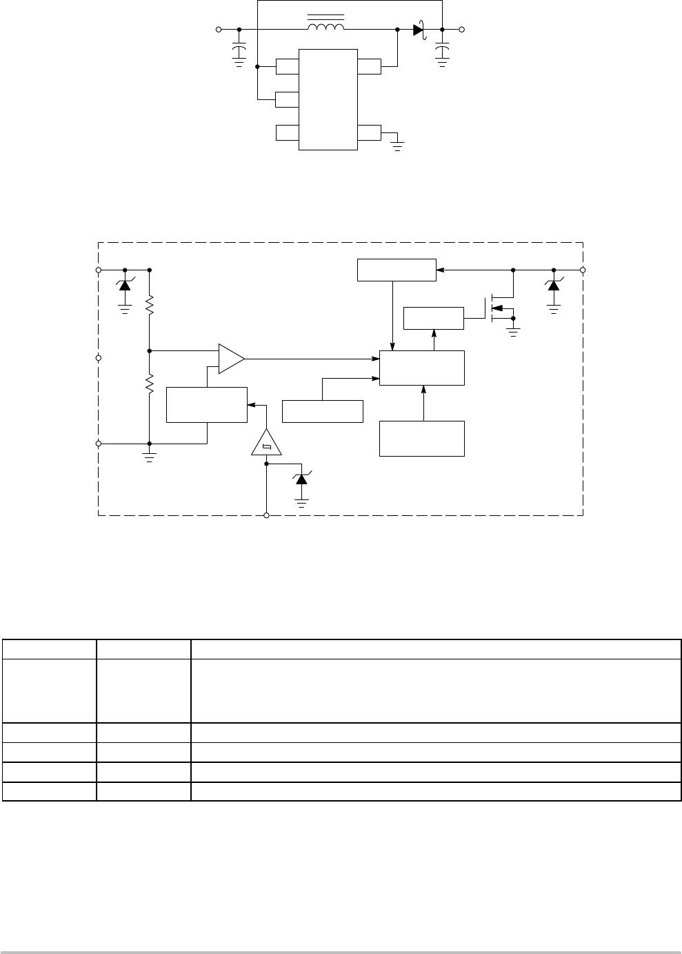
The NCP1402 series are monolithic micropower step−up DC to DC
converter that are specially designed for powering portable equipment
from one or two cell battery packs.These devices are designed to
startup with a cell voltage of 0.8 V and operate down to less than 0.3 V.
With only three external components, this series allow a simple means
to implement highly efficient converters that are capable of up to
200 mA of output current at V
in
= 2.0 V, V
OUT
= 3.0 V.
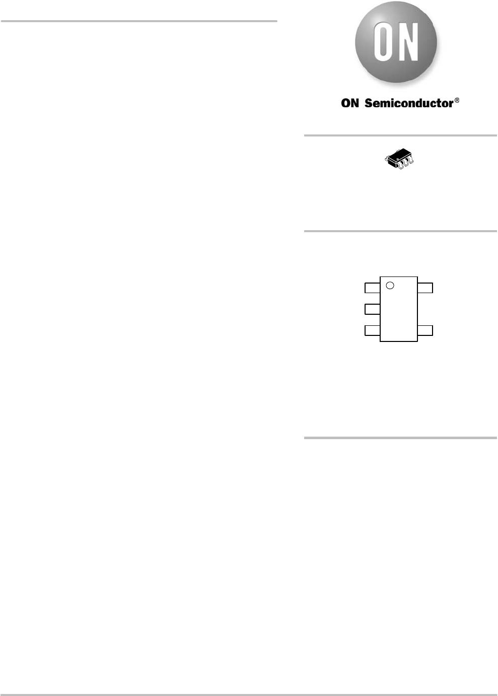
Each device consists of an on−chip PFM (Pulse Frequency
Modulation) oscillator, PFM controller, PFM comparator, soft−start,
voltage reference, feedback resistors, driver, and power MOSFET
switch with current limit protection. Additionally, a chip enable
feature is provided to power down the converter for extended battery
life.
The NCP1402 device series are available in the Thin SOT−23−5
package with five standard regulated output voltages. Additional
voltages that range from 1.8 V to 5.0 V in 100 mV steps can be
manufactured.
Features
• Extremely Low Startup Voltage of 0.8 V
• Operation Down to Less than 0.3 V
• High Efficiency 85% (V
in
= 2.0 V, V
OUT
= 3.0 V, 70 mA)
• Low Operating Current of 30 mA (V
OUT
= 1.9 V)
• Output Voltage Accuracy ±2.5%
• Low Converter Ripple with Typical 30 mV
• Only Three External Components Are Required
• Chip Enable Power Down Capability for Extended Battery Life
• Micro Miniature Thin SOT−23−5 Packages
• These Devices are Pb−Free and are RoHS Compliant
Typical Applications
• Cellular Telephones
• Pagers
• Personal Digital Assistants (PDA)
• Electronic Games
• Portable Audio (MP3)
• Camcorders
• Digital Cameras
• Handheld Instruments
ORDERING INFORMATION
SOT23−5
(TSOP−5, SC59−5)
SN SUFFIX
CASE 483
PIN CONNECTIONS AND
MARKING DIAGRAM
1
3
GND
CE
2
OUT
NC
4
LX
5
(Top View)
xxx = Marking
A = Assembly Location
Y = Year
W = Work Week
G = Pb−Free Package
See detailed ordering and shipping information in the ordering
information section on page 17 of this data sheet.
http://onsemi.com
xxxAYW G
G
(Note: Microdot may be in either location)