NCP1402
http://onsemi.com
13
2.5
1.0
3.0
1.5
2.0
3.5
0
60
604020
V
ripple
, RIPPLE VOLTAGE (mV)
0
Figure 51. NCP1402SN19T1 Ripple Voltage vs.
Output Current
Figure 52. NCP1402SN30T1 Ripple Voltage vs.
Output Current
Figure 53. NCP1402SN50T1 Ripple Voltage vs.
Output Current
Figure 54. NCP1402SNXXT1 Operating
Current 1 vs. Output Voltage
V
OUT
, OUTPUT VOLTAGE (V)
I
DD1
, OPERATING CURRENT 1 (mA)
Figure 55. NCP1402SNXXT1 Pin On−state
Current vs. Output Voltage
Figure 56. NCP1402SNXXT1 Switch−On
Resistance vs. Output Voltage
80
13425
V
in
= 1.2 V
NCP1402SN19T1
L = 47 mH
C
OUT
= 68 mF
T
A
= 25°C
85°C
I
O
, OUTPUT CURRENT (mA)
20
40
100
80 100 120 140 160 180 200
V
in
= 0.9 V
V
in
= 1.5 V
0
60
604020
V
ripple
, RIPPLE VOLTAGE (mV)
0
80
V
in
= 1.2 V
NCP1402SN30T1
L = 47 mH
C
OUT
= 68 mF
T
A
= 25°C
I
O
, OUTPUT CURRENT (mA)
20
40
100
80 100 120 140 160 180 20
0
V
in
= 0.9 V
V
in
= 1.5 V
0
60
604020
V
ripple
, RIPPLE VOLTAGE (mV)
0
80
V
in
= 1.2 V
NCP1402SN50T1
L = 47 mH
C
OUT
= 68 mF
T
A
= 25°C
I
O
, OUTPUT CURRENT (mA)
20
40
100
80 100 120 140 160 180 200
V
in
= 0.9 V
V
in
= 1.5 V
V
in
= 2.0 V
V
in
= 2.5 V
V
in
= 2.0 V
V
in
= 3.0 V
V
in
= 4.0 V
60
0
80
20
40
100
6
25°C
−40°C
NCP1402SNXXT1
V
OUT
= V
SET
x 0.96
Open−loop Test
V
OUT
, OUTPUT VOLTAGE (V)
R
DS(ON)
, SWITCH−ON RESISTANCE (W)
13425
85°C
6
25°C
−40°C
NCP1402SNXXT1
V
OUT
= V
SET
x 0.96
V
LX
= 0.4 V
Open−loop Test
V
OUT
, OUTPUT VOLTAGE (V)
I
LX
, LX PIN ON−STATE CURRENT (mA)
13425
85°C
220
100
260
140
180
300
6
25°C
−40°C
NCP1402SNXXT1
V
OUT
= V
SET
x 0.96
V
LX
= 0.4 V
Open−loop Test
NCP1402
http://onsemi.com
14
300
200
0
400
0
125
321
I
in(no
load)
, NO LOAD INPUT CURRENT (mA)
0
V
in
, INPUT VOLTAGE (V)
Figure 57. NCP1402SNXXT1 No Load Input
Current vs. Input Voltage
Figure 58. NCP1402SNXXT1 Maximum Output
Current vs. Input Voltage
I
O(max)
, MAX. OUTPUT CURRENT (mA)
150
0
1.9 V
NCP1402SNXXT1
L = 47 mH
I
O
= 0 mA
T
A
= 25°C
V
in
, INPUT VOLTAGE (V)
25
50
75
100
45
100
6
2.7 V
3.0 V
3.3 V
5.0 V
1.9 V
2.7 V
3.0 V
3.3 V 5.0 V
NCP1402SNXXT1
L = 47 mH
T
A
= 25°C
12345
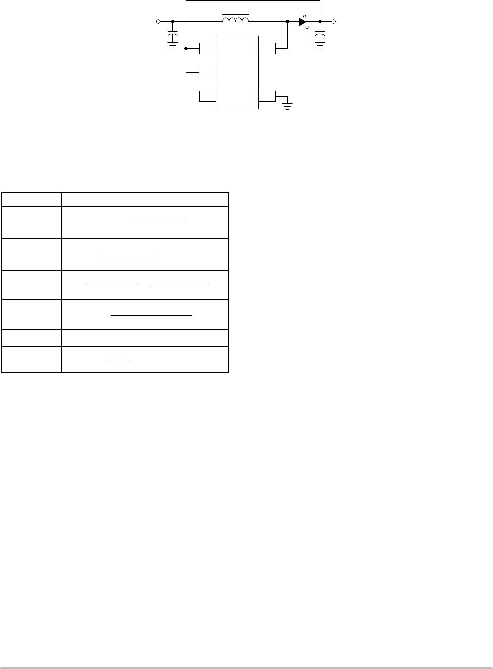
DETAILED OPERATING DESCRIPTION
Operation
The NCP1402 series are monolithic power switching
regulators optimized for applications where power drain
must be minimized. These devices operate as variable
frequency, voltage mode boost regulators and designed to
operate in continuous conduction mode. Potential
applications include low powered consumer products and
battery powered portable products.
The NCP1402 series are low noise variable frequency
voltage−mode DC−DC converters, and consist of Soft−Start
circuit, feedback resistor, reference voltage, oscillator, PFM
comparator, PFM control circuit, current limit circuit and
power switch. Due to the on−chip feedback resistor network,
the system designer can get the regulated output voltage
from 1.8 V to 5 V with a small number of external
components. The operating current is typically 30 mA
(V
OUT
= 1.9 V), and can be further reduced to about 0.6 mA
when the chip is disabled (V
CE
< 0.3 V).
The NCP1402 operation can be best understood by
examining the block diagram in Figure 2. PFM comparator
monitors the output voltage via the feedback resistor. When
the feedback voltage is higher than the reference voltage, the
power switch is turned off. As the feedback voltage is lower
than reference voltage and the power switch has been off for
at least a period of minimum off−time decided by PFM
oscillator, the power switch is then cycled on for a period of
on−time also decided by PFM oscillator, or until current
limit signal is asserted. When the power switch is on, current
ramps up in the inductor, storing energy in the magnetic
field. When the power switch is off, the energy in the
magnetic field is transferred to output filter capacitor and the
load. The output filter capacitor stores the charge while the
inductor current is high, then holds up the output voltage
until next switching cycle.
Soft−Start
There is a Soft−Start circuit in NCP1402. When power is
applied to the device, the Soft−Start circuit pumps up the
output voltage to approximately 1.5 V at a fixed duty cycle, the
level at which the converter can operate normally. What is
more, the startup capability with heavy loads is also improved.
Regulated Converter Voltage (V
OUT
)
The V
OUT
is set by an internal feedback resistor network.
This is trimmed to a selected voltage from 1.8 to 5.0 V range
in 100 mV steps with an accuracy of ±2.5%.
Current Limit
The NCP1402 series utilizes cycle−by−cycle current
limiting as a means of protecting the output switch
MOSFET from overstress and preventing the small value
inductor from saturation. Current limiting is implemented
by monitoring the output MOSFET current build−up during
conduction, and upon sensing an overcurrent conduction
immediately turning off the switch for the duration of the
oscillator cycle.
The voltage across the output MOSFET is monitored and
compared against a reference by the VLX limiter. When the
threshold is reached, a signal is sent to the PFM controller
block to terminate the power switch conduction. The current
limit threshold is typically set at 350 mA.
Enable / Disable Operation
The NCP1402 series offer IC shut−down mode by chip
enable pin (CE pin) to reduce current consumption. An
internal pullup resistor tied the CE pin to OUT pin by default
i.e. user can float the pin CE for permanent “On”. When
voltage at pin CE is equal or greater than 0.9 V, the chip will
be enabled, which means the regulator is in normal
operation. When voltage at pin CE is less than 0.3 V, the chip
is disabled, which means IC is shutdown.
Important: DO NOT apply a voltage between 0.3 V and 0.9 V to pin CE as this is the CE pin’s hyteresis voltage
range. Clearly defined output states can only be obtained by applying voltage out of this range.
NCP1402
http://onsemi.com
15
APPLICATIONS CIRCUIT INFORMATION
1
3
GND
CE
2
OUT
NC
4
LX
5
NCP1402
Figure 59. Typical Application Circuit
V
OUT
C2
68 mF
D1
L1
47 mH
C1
10 mF
V
in
Step−up Converter Design Equations
NCP1402 step−up DC−DC converter designed to operate
in continuous conduction mode can be defined by:
Calculation Equation
L
v M
ǒ
V
in
2
V
OUT
I
Omax
Ǔ
I
PK
(V
in
* V
s)
t
on
L
) I
min
I
min
(t
on
) t
off
)I
O
t
off
*
(V
in
* V
S
)t
on
2L
t
off
(V
in
* V
s)
t
on
(V
OUT
) V
F
* V
in
)
DQ
(I
L
* I
O
)t
off
V
ripple
[
DQ
C
OUT
) (I
L
* I
O
)ESR
*NOTES:
I
PK
Peak inductor current
I
min
Minimum inductor current
I
O
Desired dc output current
I
Omax
Desired maximum dc output current
I
L
Average inductor current
V
in
Nominal operating dc input voltage
V
OUT
Desired dc output voltage
V
F
Diode forward voltage
V
S
Saturation voltage of the internal FET switch
DQ Charge stores in the C
OUT
during charging up
V
ripple
Output ripple voltage
ESR Equivalent series resistance of the output capacitor
M An empirical factor, when V
OUT
3.0 V,
M = 8 x 10
−6
, otherwise M = 5.3 x 10
−6
.
EXTERNAL COMPONENT SELECTION
Inductor
The NCP1402 is designed to work well with a 47 mH
inductor in most applications. 47 mH is a sufficiently low
value to allow the use of a small surface mount coil, but large
enough to maintain low ripple. Low inductance values
supply higher output current, but also increase the ripple and
reduce efficiency. Note that values below 27 mH is not
recommended due to NCP1402 switch limitations. Higher
inductor values reduce ripple and improve efficiency, but
also limit output current.
The inductor should have small DCR, usually less than 1 W
to minimize loss. It is necessary to choose an inductor with
saturation current greater than the peak current which the
inductor will encounter in the application.
Diode
The diode is the main source of loss in DC−DC converters.
The most importance parameters which affect their
efficiency are the forward voltage drop, V
F
, and the reverse
recovery time, t
rr
. The forward voltage drop creates a loss
just by having a voltage across the device while a current
flowing through it. The reverse recovery time generates
a loss when the diode is reverse biased, and the current
appears to actually flow backwards through the diode due to
the minority carriers being swept from the P−N junction.
A Schottky diode with the following characteristics is
recommended:
Small forward voltage, V
F
< 0.3 V
Small reverse leakage current
Fast reverse recovery time/ switching speed
Rated current larger than peak inductor current,
I
rated
> I
PK
Reverse voltage larger than output voltage,
V
reverse
> V
OUT
Input Capacitor
The input capacitor can stabilize the input voltage and
minimize peak current ripple from the source. The value of
the capacitor depends on the impedance of the input source
used. Small Equivalent Series Resistance (ESR) Tantalum or
ceramic capacitor with value of 10 mF should be suitable.

NCP1402SN19T1G

Mfr. #:
Manufacturer:
ON Semiconductor
Description:
Switching Voltage Regulators 1.9V 200mA Boost PWM
Lifecycle:
New from this manufacturer.
Delivery:
DHL FedEx Ups TNT EMS
Payment:
T/T Paypal Visa MoneyGram Western Union