NCP1402
http://onsemi.com
4
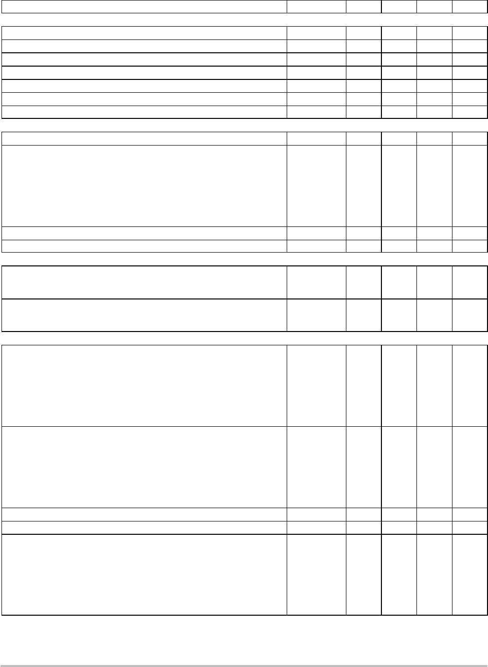
ELECTRICAL CHARACTERISTICS (For all values T
A
= 25°C, unless otherwise noted.)
Characteristic
Symbol Min Typ Max Unit
OSCILLATOR
Switch On Time (current limit not asserted)
t
on
3.6 5.5 7.6
ms
Switch Minimum Off Time t
off
1.0 1.45 1.9
ms
Maximum Duty Cycle D
MAX
70 78 85 %
Minimum Startup Voltage (I
O
= 0 mA) V
start
− 0.8 0.95 V
Minimum Startup Voltage Temperature Coefficient (T
A
= −40°C to 85°C)
DV
start
− −1.6 − mV/°C
Minimum Operation Hold Voltage (I
O
= 0 mA) V
hold
0.3 − − V
Soft−Start Time (V
OUT
u 0.8 V) t
SS
0.3 2.0 − ms
LX (PIN 5)
Internal Switching N−Channel FET Drain Voltage
V
LX
− − 6.0 V
LX Pin On−State Sink Current (V
LX
= 0.4 V)
Device Suffix:
19T1
27T1
30T1
33T1
40T1
50T1
I
LX
110
130
130
130
130
130
145
180
190
200
210
215
−
−
−
−
−
−
mA
Voltage Limit V
LXLIM
0.45 0.65 0.9 V
Off−State Leakage Current (V
LX
= 6.0 V, T
A
= −40°C to 85°C) I
LKG
− 0.5 1.0
mA
CE (PIN 1)
CE Input Voltage (V
OUT
= V
SET
x 0.96)
High State, Device Enabled
Low State, Device Disabled
V
CE(high)
V
CE(low)
0.9
−
−
−
−
0.3
V
CE Input Current (Note 6)
High State, Device Enabled (V
OUT
= V
CE
= 6.0 V)
Low State, Device Disabled (V
OUT
= 6.0 V, V
CE
= 0 V)
I
CE(high)
I
CE(low)
−0.5
−0.5
0
0.15
0.5
0.5
mA
TOTAL DEVICE
Output Voltage
Device Suffix:
19T1
27T1
30T1
33T1
40T1
50T1
V
OUT
1.853
2.632
2.925
3.218
3.900
4.875
1.9
2.7
3.0
3.3
4.0
5.0
1.948
2.768
3.075
3.383
4.100
5.125
V
Output Voltage Temperature Coefficient (T
A
= −40°C to +85°C)
Device Suffix:
19T1
27T1
30T1
33T1
40T1
50T1
DV
OUT
−
−
−
−
−
−
150
150
150
150
150
150
−
−
−
−
−
−
ppm/°C
Operating Current 2 (V
OUT
= V
CE
= V
SET
+0.5 V, Note 5) I
DD2
− 13 15
mA
Off−State Current (V
OUT
= 5.0 V, V
CE
= 0 V, T
A
= −40°C to +85°C, Note 6) I
OFF
− 0.6 1.0
mA
Operating Current 1 (V
OUT
= V
CE
= V
SET
x 0.96)
Device Suffix:
19T1
27T1
30T1
33T1
40T1
50T1
I
DD1
−
−
−
−
−
−
30
39
42
45
55
70
50
60
60
60
100
100
mA
Product parametric performance is indicated in the Electrical Characteristics for the listed test conditions, unless otherwise noted. Product
performance may not be indicated by the Electrical Characteristics if operated under different conditions.
5. V
SET
means setting of output voltage.
6. CE pin is integrated with an internal 10 MW pullup resistor.

