LTC3626
11
3626fa
For more information www.linear.com/LTC3626
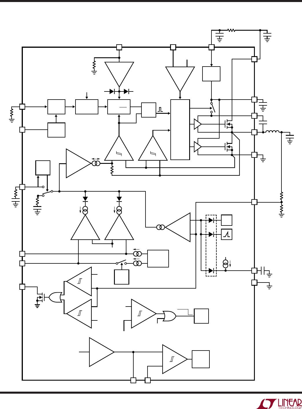
operaTion
The LTC3626 is a current mode, monolithic, step-down
regulator capable of providing up to 2.5A of output current
from an input supply as high as 20V. Its unique controlled
on-time architecture allows extremely low step-down ratios
while maintaining a constant switching frequency. The part
is enabled by raising the RUN pin above 1.25V (typical).
Main Control Loop
In normal operation the internal top power MOSFET is
turned on for a fixed interval determined by an internal
one-shot timer (“ON” signal in the Functional Diagram).
When the top power MOSFET turns off, the bottom power
MOSFET turns on until the current comparator, I
CMP
, trips,
thus restarting the one-shot timer and initiating the next
cycle. The inductor current is monitored by sensing the
voltage drop across the bottom power MOSFET. The volt
-
age at the ITH node sets the I
CMP
comparator threshold
corresponding to the inductor valley current. The error
amplifier, EA, adjusts the ITH voltage by comparing an
internal 0.6V reference voltage to the feedback signal, V
FB
,
derived from the output voltage. If, for example, the load
current increases, the output voltage will decrease relative
to the 0.6V reference. The ITH voltage then rises until the
average inductor current matches that of the load current.
At light load currents the inductor current can drop to
zero or become negative. If the LTC3626 is configured for
Burst Mode operation, this inductor current condition is
detected by the current reversal comparator, I
REV
, which
in turn shuts off the bottom power MOSFET and places
the part into a low quiescent current sleep state resulting
in discontinuous operation and increased efficiency at low
load currents. Both power MOSFETs remain off with the
part in sleep and the output capacitor supplying the load
current until the ITH voltage rises sufficiently to initiate
another cycle. Discontinuous operation is disabled by
tying the MODE/SYNC pin to ground, placing the LTC3626
into forced continuous mode
. In forced continuous mode,
continuous synchronous operation occurs regardless of
the output load current.
The operating frequency is determined by the value of the R
T
resistor, which programs the current for the internal oscil-
lator. An internal phase-locked loop adjusts the switching
regulator on-time to track the internal oscillator edge and
for
ce a constant switching frequency
, subject to t
ON
and
t
OFF
time constraints as shown in the Electrical Character-
istics table. Alternatively, the RT pin can be connected to
the INTV
CC
pin which causes the internal oscillator to run
at the default frequency of 2MHz. Finally, a clock signal
can be applied to the MODE/SYNC pin to synchronize the
switching frequency to an external source. The regulator
defaults to forced continuous operation when an external
clock signal is applied.
Output/Input Current Monitor and Limit
The LTC3626 provides a scaled replica of the average
output current and a scaled replica of the average input
current at the IMON
OUT
and IMON
IN
pins respectively. The
average current at each of these pins will be 1/16,000th
of the measured average current. Further, the voltage at
each pin is continuously fed to independent current limit
amplifiers that have a voltage reference at 1.2V. Thus, a
programmable average current limit for the output current
and/or input current may be obtained by placing a resistor
of suitable value at the pin of interest so as to produce
1.2V at the desired current limit. When the current limit
feature is used, a compensation capacitor (1µF typical)
should be placed in parallel with the chosen resistor. The
output or input current monitor and limit circuits may be
individually disabled by pulling IMON
OUT
or IMON
IN
to
INTV
CC
as appropriate.