LTC3626
4
3626fa
For more information www.linear.com/LTC3626
elecTrical characTerisTics
The l denotes the specifications which apply over the specified operating
junction temperature range, otherwise specifications are at T
A
= 25°C (Note 3). PV
IN
= SV
IN
=
12V unless otherwise specified.
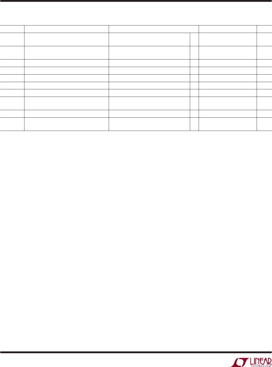
SYMBOL PARAMETER CONDITIONS MIN TYP MAX UNITS
PGOOD Good-to-Bad Threshold FB Rising
FB Falling
8
–8
10
–10
%
%
PGOOD Bad-to-Good Threshold FB Rising
FB Falling
–3
3
–5
5
%
%
Power Good Filter Time 20
40 μs
R
PGOOD
PGOOD Pull-Down Resistance 10mA Load 20 Ω
Switch Leakage Current V
RUN
= 0V 0.01 1 μA
t
SS
Internal Soft-Start Time V
FB
from 10% to 90% Full Scale 400 700 μs
I
TRACK/SS
TRACK/SS Pull-Up Current 1.4 μA
MODE Threshold Voltage MODE V
IH
MODE V
IL
l
l
1.0
0.4
V
V
SYNC Threshold Voltage SYNC V
IH
l
1.4 V
MODE Input Current MODE = 0V
MODE = INTV
CC
–1.5
1.5
μA
µA
Note 1:
Stresses beyond those listed under Absolute Maximum Ratings
may cause permanent damage to the device. Exposure to any Absolute
Maximum Rating condition for extended periods may affect device
reliability and lifetime.
Note 2: Guaranteed by long term current density limitations.
Note 3: The LTC3626 is tested under pulsed load conditions such that
T
J
≈ T
A
. The LTC3626E is guaranteed to meet performance specifications
from 0°C to 85°C. Specifications over the –40°C to 125°C operating
junction temperature range are assured by design, characterization, and
correlation with statistical process controls. The LTC3626I is guaranteed
over the –40°C to 125°C operating junction temperature range. Note that
the maximum ambient temperature consistent with these specifications
is determined by specific operating conditions in conjunction with board
layout, the rated package thermal impedance, and other environmental
factors.
Note 4: This IC includes overtemperature protection that is intended to
protect the device during momentary overload conditions. The maximum
rated junction temperature will be exceeded when this protection is active.
Continuous operation above the specified absolute maximum operating
junction temperature may impair device reliability or permanently damage
the device.
Note 5: Output voltages above 6V are not optimized for controlled
on-time operation. Refer to the Applications Information section for
further discussions related to the output voltage range. Verified at test by
comparison of measured on-time to V
ON
voltage.
Note 6: Tested in a proprietary test mode, where I
SW
flows through the
synchronous switch only.
Note 7: Guaranteed by design.
Note 8: Maximum allowed current draw when used as a regulated output
is 5mA. This supply is only intended to supply additional DC load currents
as needed and not intended to regulate large transient or AC behavior as
these waveforms may impact LTC3626 operation.
LTC3626
5
3626fa
For more information www.linear.com/LTC3626
Typical perForMance characTerisTics
Efficiency vs Input Voltage
(Burst Mode Operation)
Efficiency vs Frequency (Forced
Continuous Mode Operation)
Reference Voltage
vs Temperature
Internal MOSFET R
DS(ON)
vs Temperature
Temperature Monitor
vs Temperature
Efficiency vs Load Current
(Burst Mode Operation)
Efficiency vs Load Current (Forced
Continuous Mode Operation)
Efficiency vs Load Current
(Burst and Forced Continuous)
LOAD CURRENT (mA)
30
EFFICIENCY (%)
90
100
20
10
80
50
70
60
40
1 100 1000 10000
3626 G01
0
10
V
IN
= 4V
V
IN
= 8V
V
IN
= 12V
V
IN
= 20V
V
OUT
= 1.8V
LOAD CURRENT (mA)
30
EFFICIENCY (%)
90
100
20
10
80
50
70
60
40
1 100 1000 10000
3626 G02
0
10
V
IN
= 4V
V
IN
= 8V
V
IN
= 12V
V
IN
= 20V
V
OUT
= 1.8V
LOAD CURRENT (mA)
30
EFFICIENCY (%)
90
100
20
10
80
50
70
60
40
1 100 1000 10000
3626 G02
0
10
V
OUT
= 5V
V
OUT
= 3.3V
Burst Mode OPERATION
FORCED
CONTINUOUS
MODE OPERATION
INPUT VOLTAGE (V)
4
EFFICIENCY (%)
80
85
90
20
3626 G04
75
70
60
8
12
16
6 22
10
14
18
65
100
95
I
LOAD
= 1A
I
LOAD
= 2.5A
I
LOAD
= 100mA
I
LOAD
= 10mA
V
OUT
= 1.8V
LOAD CURRENT (mA)
30
EFFICIENCY (%)
90
100
20
10
80
50
70
60
40
1 100 1000 10000
3626 G05
0
10
f = 500kHz
f = 1MHz
f = 2MHz
f = 3MHz
V
OUT
= 3.3V
TEMPERATURE (°C)
–50
V
FB
(V)
0.602
0.604
0.606
25 75
3626 G06
0.600
0.598
–25 0
50 100 125
0.596
0.594
TEMPERATURE (°C)
–50
R
DS(ON)
(mΩ)
140
25
3626 G07
80
40
–25 0 50
20
0
160
120
100
60
75 100 125
TOP SWITCH
BOTTOM SWITCH
TEMPERATURE (°C)
–50
50
75
125
25 75
3626 G08
25
0
–25 0
50 100 125
–25
–50
100
1.6
1.7
2.0
1.5
1.4
1.2
1.1
1.9
MEASURED TEMPERATURE (°C)
TEMPERATURE MONITOR VOLTAGE (V)
T
A
= 25°C, PV
IN
= SV
IN
= 12V, f = 1MHz unless otherwise noted.
LTC3626
6
3626fa
For more information www.linear.com/LTC3626
Typical perForMance characTerisTics
Quiescent Current vs V
IN
(Burst Mode Operation)
Oscillator Frequency
vs Temperature
Oscillator Internal Set Frequency
vs Temperature
TRACK/SS Pull-Up Current
vs Temperature
Output Current Monitor Error
vs Output Current
Input Current Monitor
vs Input Current
Input Current Monitor Error
vs Input Current
Output Current Monitor
vs Output Current
OUTPUT CURRENT (A)
0.5
CALCULATED OUTPUT CURRENT,
IMON
OUT
• 16000 (A)
IMON
OUT
CURRENT (µA)
1.50
2.00
2.5
3626 G09
1.00
0.50
1.0
1.5
2.0
0.75
1.25
1.75
2.25
2.50
94
125
63
31
156
1.25
1.75
0.75
2.25
T
A
= 85°C
T
A
= 25°C
T
A
= –40°C
OUTPUT CURRENT (A)
1
–5
MEASURED OUTPUT CURRENT ERROR (%)
–3
–1
1
1.25
1.5
1.75 2
2.25
3
5
–4
–2
0
2
4
2.5
T
A
= 85°C
T
A
= 25°C
T
A
= –40°C
INPUT CURRENT (A)
0.1
CALCULATED INPUT CURRENT,
IMON
IN
• 16000 (A)
IMON
IN
CURRENT (µA)
0.30
0.40
0.5
3626 G11
0.20
0.10
0.2
0.3
0.4
0.15
0.25
0.35
0.45
0.50
19
25
13
6
31
16
22
9
28
0.25
0.35
0.15
0.45
T
A
= 85°C
T
A
= 25°C
T
A
= –40°C
INPUT CURRENT (A)
0.16
–10
MEASURED INPUT CURRENT ERROR (%)
–8
–4
–2
0
10
4
0.24
0.32
0.36
3626 G12
–6
6
8
2
0.20 0.28
0.40
0.44
0.48
T
A
= 85°C
T
A
= 25°C
T
A
= –40°C
INPUT VOLTAGE (V)
4
I
Q
(µA)
300
400
20
3626 G13
200
100
8
12
16
6
10
14
18
500
250
350
150
450
T
A
= 85°C
T
A
= 25°C
T
A
= –40°C
TEMPERATURE (°C)
50
–10
FREQUENCY VARIATION (%)
–8
–4
–2
0
10
4
0
50
75 100
3626 G14
–6
6
8
2
25
25
125
R
T
= 158kΩ
TEMPERATURE (°C)
–50
FREQUENCY (MHz)
2.2
2.4
2.6
25 75
3626 G15
2.0
1.8
–25 0
50 100 125
1.6
1.4
R
T
= INTV
CC
TEMPERATURE (°C)
–50
1.4
1.6
2.0
25 75
3626 G16
1.2
1.0
–25 0
50 100 125
0.8
0.6
1.8
I
TRACK/SS
(µA)
T
A
= 25°C, PV
IN
= SV
IN
= 12V, f = 1MHz unless otherwise noted.

LTC3626EUDC#PBF

Mfr. #:
Manufacturer:
Analog Devices / Linear Technology
Description:
Switching Voltage Regulators 3A, 20V Monolithic Step-Down Regulator with Current and Temperature Monitoring
Lifecycle:
New from this manufacturer.
Delivery:
DHL FedEx Ups TNT EMS
Payment:
T/T Paypal Visa MoneyGram Western Union