LTC3626
22
3626fa
For more information www.linear.com/LTC3626
applicaTions inForMaTion
From the previous section, I
GATECHG
is approximately 5mA
when f = 2MHz, and the spec table lists the typical I
Q
to be
approximately 1mA. Therefore, the total power dissipation
due to resistive losses and LDO losses is:
P
D
= I
OUT
2
R
SW
+ V
IN
(I
GATECHG
+ I
Q
)
P
D
= (2.5A)
2
(0.092Ω) + 12V 5mA = 635mW
The QFN 3mm × 4mm package junction-to-ambient thermal
resistance, θ
JA
, is approximately 47°C/W. Therefore, the
junction temperature of the regulator operating in a 70°C
ambient temperature is approximately:
T
J
= 0.63W 47°C/W + 70°C = 100°C
which is below the maximum junction temperature of
125°C.
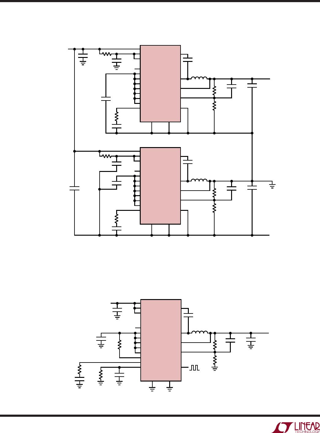
Board Layout Considerations
When laying out the printed circuit board, the following
checklist should be used to ensure proper operation of
the LTC3626.
1. Does the capacitor C
IN
connect to PV
IN
and PGND as
close to the pins as possible? These capacitors provide
the AC current to the internal power MOSFETs. The (–)
plate of C
IN
should be closely connected to PGND and
the (–) plate of C
OUT
.
2. The output capacitor, C
OUT
, and inductor L1 should
be closely connected to minimize loss. The (–) plate
of C
OUT
should be closely connected to PGND and the
(–) plate of C
IN
.
3. The resistive divider, R1 and R2, must be connected
between the (+) plate of C
OUT
and a ground line termi-
nated near SGND. The feedback signal, V
FB
, should be
routed away from noisy components and traces such as
the SW and BOOST lines, and its trace length should be
minimized. In addition, RT, compensation components,
and current and temperature monitor/limit components
should be terminated to SGND.
4. Keep sensitive components away from the SW and
BOOST pins. The R
RT
resistor, the feedback resistors,
the compensation components, the current monitor
components, and the INTV
CC
bypass capacitor should
all be routed away from the SW trace and the inductor.
5. A ground plane is preferred, but if not available the
signal and power grounds should be segregated with
both connecting to a common, low noise reference
point. The point at which the ground terminals of the
V
IN
and V
OUT
bypass capacitors are connected makes a
good, low noise reference point. The connection to the
PGND pin should be made with a minimal resistance
trace from the reference point.
6. Flood all unused areas on all layers with copper in order
to reduce the temperature rise of power components.
These copper areas should be connected to the exposed
backside connection of the IC.
Design Example
As a design example, consider using the LTC3626 in an
application with the following specifications:
V
IN
= 12V, V
OUT
= 1.8V, I
OUT(MAX)
= 2.5A, I
OUT(MIN)
=
50mA
Further, the ability to continuously monitor the average
output current (I
OUT
) and the internal temperature is de-
sired. Finally, an average I
OUT
limit of 2.5A and an internal
temperature limit of approximately 125°C are desired.
Because efficiency is important at both high and low load
currents, Burst Mode operation and 1MHz operation is
chosen.
First, the correct R
RT
resistor value for 1MHz switching
frequency must be chosen. Based on the equation in the
Applications Information section, R
RT
is calculated to be
320k. A standard 324k resistor is selected for R
RT
.
LTC3626
23
3626fa
For more information www.linear.com/LTC3626
applicaTions inForMaTion
Next, determine the inductor value for approximately 40%
ripple current using:
L =
1.8V
1MHz 1A
1
1.8V
12V
= 1.53µH
A standard 1.5µH inductor will work well for this application.
Next, C
OUT
is selected based on the required output tran-
sient performance and the required ESR to satisfy the
output voltage ripple.
For this design, two 22µF ceramic
capacitors will be used.
C
IN
should be sized for a maximum current rating of:
I
RMS
= 2.5A
1.8V 12V 1.8V
( )
12V
= 0.89
A
Decoupling the PV
IN
pin with a 47µF ceramic capacitor
should be adequate for most applications. An additional
F capacitor on the PV
IN
can be used to help reduce
ringing as required. A 0.33µF capacitor on the SV
IN
pin is
optional and will be tied to PV
IN
through a resistor for
additional filtering at the SV
IN
pin. Finally, a 0.1µF boost
capacitor should work for most applications.
To save board space, the ITH pin is connected to INTV
CC
to select the internal compensation network.
The PGOOD pin is connected to V
IN
through a 100k resis-
tor to INTV
CC
.
To program the I
OUT
limit at 2.5A, a resistor is connected
between IMON
OUT
and SGND with a desired value equal to:
R
IOUT
=
16,000 1.2V
2.5A
= 7.68k
W
Thus, a standard 7.68kΩ will be selected for R
IOUT
. A 1µF
capacitor placed in parallel with R
IOUT
for I
OUT
limit loop
compensation should be adequate for most applications.
The 125°C temperature limit is programmed by setting a
voltage at the TSET pin equal to:
V
TSET
=
125
°
C
+
273
200
°
K/V
2V
In this example, the TSET voltage will be derived by divid-
ing the available INTV
CC
voltage using R
TSET1
= 432k and
R
TSET2
= 665k.
PV
IN
SV
IN
RUN
BOOST
SW
V
ON
FB
RT
INTV
CC
TRACK/SS
ITH
MODE/SYNC
IMON
IN
PGOOD
TMON
TSET
IMON
OUT
SGND PGND
LTC3626
C
IN2
F
C
IN1
47µF
R3
C3
0.33µF
V
OUT
1.8V
2.5A
V
IN
12V
R
IOUT
7.68k
C
IOUT
F
C
INTVCC
2.2µF
C
BST
0.1µF
C
F
22pF
C
OUT
47µF
L1
1.5µH
R
TSET2
665k
R
TSET1
432k
R1
40.2k
R2
20k
R
PGD
100k
3626 F07
R
T
324k
Figure 7. 12V Input to 1.8V Output, 2.5A Regulator at 1MHz in Burst Mode Operation with
Output Current Monitor and 2.5A Limit, On-Die Temperature Monitor and 125°C Limit
LTC3626
24
3626fa
For more information www.linear.com/LTC3626
Typical applicaTions
12V Input to ±5V Output at 2MHz
5V Input to 2.5V Output at 1MHz Synchronized Frequency with
Input Current Monitor and 475mA Input Current Limit
PV
IN
SV
IN
RUN
BOOST
SW
V
ON
FB
INTV
CC
RT
TSET
IMON
OUT
TMON
PGOOD
ITH
IMON
IN
SGND PGND
LTC3626
C1
47µF
V
OUT
2.5V
2.5A
V
IN
5V
C
COMP
220pF
C4
2.2µF
C
IIN
F
C
BST
0.1µF
C
F
22pF
C
OUT
47µF
L1
2.2µH
R
IIN
40.2k
R
COMP
13k
R1
127k
R2
40.2k
EXTERNAL
CLOCK
R
PGD
100k
3626 TA03
TRACK/SS
MODE/SYNC
PV
IN
SV
IN
RUN
BOOST
SW
V
ON
FB
MODE/SYNC
PGOOD
INTV
CC
RT
TSET
TMON
IMON
IN
IMON
OUT
TRACK/SS
ITH
SGND PGND
LTC3626
C1
47µF
R3A
C3A
0.33µF
V
OUT
5V
2.5A
V
IN
12V
C
COMPA
220pF
C4A
2.2µF
C
BSTA
0.1µF
C
FA
22pF
C
OUTA
47µF
L1A
1.5µH
R
COMPA
13k
R1A
294k
R2A
40.2k
PV
IN
SV
IN
RUN
BOOST
SW
V
ON
FB
MODE/SYNC
PGOOD
INTV
CC
RT
TSET
TMON
IMON
IN
IMON
OUT
TRACK/SS
ITH
SGND PGND
LTC3626
R3B
C3B
0.33µF
V
OUT
–5V
1.2A
C
COMPB
220pF
C4B
2.2µF
C
BSTB
0.1µF
C
FB
22pF
C
OUTB
47µF
L1B
1.5µH
R
COMPB
13k
R1B
294k
R2B
40.2k
C1B
47µF

LTC3626EUDC#PBF

Mfr. #:
Manufacturer:
Analog Devices / Linear Technology
Description:
Switching Voltage Regulators 3A, 20V Monolithic Step-Down Regulator with Current and Temperature Monitoring
Lifecycle:
New from this manufacturer.
Delivery:
DHL FedEx Ups TNT EMS
Payment:
T/T Paypal Visa MoneyGram Western Union