AD830
Rev. C | Page 11 of 20
THEORY OF OPERATION
TRADITIONAL DIFFERENTIAL AMPLIFICATION
In the past, when differential amplification was needed to reject
common-mode signals superimposed with a desired signal,
most often the solution used was the classic op amp based
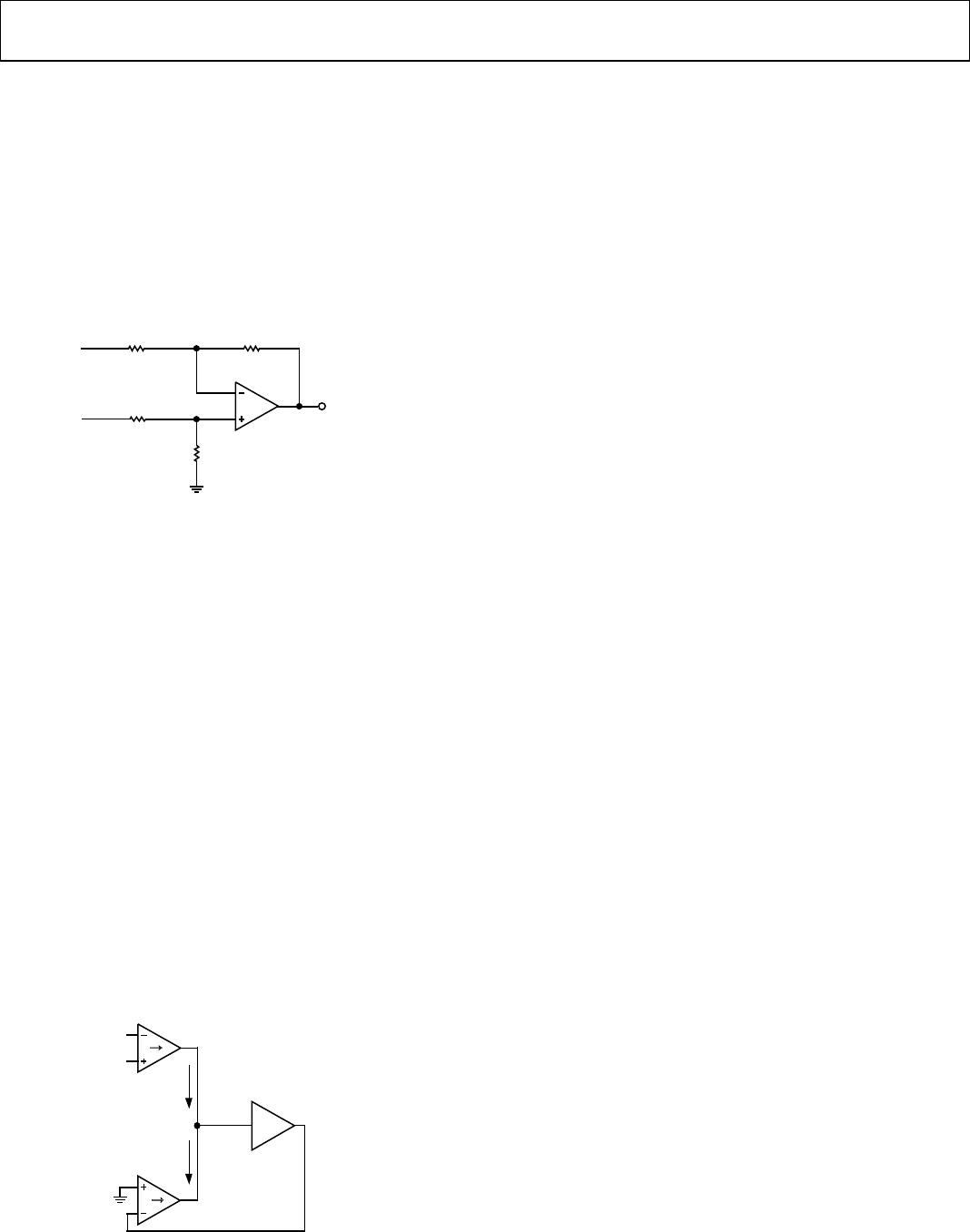
difference amplifier shown in Figure 24. The basic function
V
O
= V
1
− V
2
is simply achieved, but the overall performance is
poor and the circuit possesses many serious problems that make
it difficult to realize a robust design with moderate to high
levels of performance.
V
1
V
OUT
2
R
1
R
2
R
3
R
4
ONLY IF R
1
= R
2
= R
3
= R
4
DOES V
OUT
= V
1
– V
2
00881-024
Figure 24. Op Amp Based Difference Amplifier
PROBLEMS WITH THE OP AMP BASED APPROACH
• Low common-mode rejection ratio (CMRR)
• Low impedance inputs
• CMRR highly sensitive to the value of source R
• Different input impedance for the + and − input
• Poor high frequency CMRR
• Requires very highly matched resistors, R
1
to R
4
, to achieve
high CMRR
• Halves the bandwidth of the op amp
• High power dissipation in the resistors for large common-
mode voltage
AD830 FOR DIFFERENTIAL AMPLIFICATION
The AD830 amplifier was specifically developed to solve the
listed problems with the discrete difference amplifier approach.
Its topology, discussed in detail in the Understanding the AD830
To p o l o g y section, by design acts as a difference amplifier. The
circuit of Figure 25 shows how simply the AD830 is configured
to produce the difference of the two signals, V
1
and V
2
, in which
the applied differential signal is exactly reproduced at the
output relative to a separate output common. Any common-
mode voltage present at the input is removed by the AD830.
V
1
V
OUT
I
Y
I
X
V
2
A = 1
V I
→
V I
→
V
OUT
= V
1
– V
2
00881-025
Figure 25. AD830 as a Difference Amplifier
ADVANTAGEOUS PROPERTIES OF THE AD830
• High common-mode rejection ratio (CMRR)
• High impedance inputs
• Symmetrical dynamic response for +1 and −1 Gain
• Low sensitivity to the value of source R
• Equal input impedance for the + and − input
• Excellent high frequency CMRR
• No halving of the bandwidth
• Constant power distortion versus common-mode voltage
• Highly matched resistors not needed
UNDERSTANDING THE AD830 TOPOLOGY
The AD830 represents Analog Devices first amplifier product to
embody a powerful alternative amplifier topology. Referred to
as active feedback, the topology used in the AD830 provides
inherent advantages in the handling of differential signals,
differing system commons, level shifting, and low distortion,
high frequency amplification. In addition, it makes possible the
implementation of many functions not realizable with single op
amp circuits or superior to op amp based equivalent circuits.
With this in mind, it is important to understand the internal
structure of the AD830.
The topology, reduced to its elemental form, is shown in Figure 26.
Nonideal effects, such as nonlinearity, bias currents, and limited
full scale, are omitted from this model for simplicity but are
discussed later. The key feature of this topology is the use of
two, identical voltage-to-current converters, G
M
, that make up
input and feedback signal interfaces. They are labeled with
inputs V
X
and V
Y
, respectively. These voltage-to-current
converters possess fully differential inputs, high linearity, high
input impedance, and wide voltage range operation. This
enables the part to handle large amplitude differential signals; it
also provides high common-mode rejection, low distortion, and
negligible loading on the source. The label, G
M
, is meant to
convey that the transconductance is a large signal quantity,
unlike in the front end of most op amps. The two G
M
stage
current outputs, I
X
and I
Y
, sum together at a high impedance
node, which is characterized by an equivalent resistance and
capacitance connected to an ac common. A unity voltage gain
stage follows the high impedance node to provide buffering
from loads. Relative to either input, the open-loop gain, A
OL
, is
set by the transconductance, G
M
, working into the resistance,
R
P
; A
OL
= G
M
× R
P
. The unity gain frequency, ω
0 dB
, for the open-
loop gain is established by the transconductance, G
M
, working
into the capacitance, C
C
; ω
0
dB
= G
M
/C
C
. The open-loop
description of the AD830 is shown below for completeness.