AD830
Rev. C | Page 7 of 20
ABSOLUTE MAXIMUM RATINGS
Table 3.
Parameter Rating
Supply Voltage ±18 V
Internal Power Dissipation
Observe derating
curves
Output Short-Circuit Duration
Observe derating
curves
Common-Mode Input Voltage ±V
S
Differential Input Voltage ±V
S
Storage Temperature Range (Q) −65°C to +150°C
Storage Temperature Range (N) −65°C to +125°C
Storage Temperature Range (RN) −65°C to +125°C
Operating Temperature Range
AD830J 0°C to +70°C
AD830A −40°C to +85°C
AD830S −55°C to +125°C
Lead Temperature Range (Soldering 60 sec) 300°C
Stresses above those listed under Absolute Maximum Ratings
may cause permanent damage to the device. This is a stress
rating only; functional operation of the device at these or any
other conditions above those indicated in the operational
section of this specification is not implied. Exposure to absolute
maximum rating conditions for extended periods may affect
device reliability.
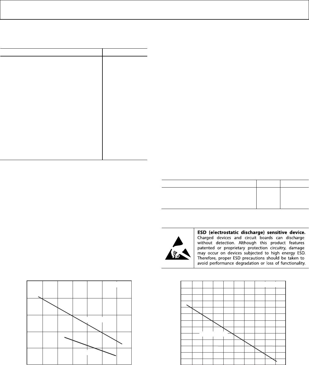
MAXIMUM POWER DISSIPATION
The maximum power that can be safely dissipated by the
AD830 is limited by the associated rise in junction temperature.
For the plastic packages, the maximum safe junction
temperature is 145°C. For the CERDIP, the maximum junction
temperature is 175°C. If these maximums are exceeded
momentarily, proper circuit operation will be restored as soon
as the die temperature is reduced. Leaving the AD830 in the
overheated condition for an extended period can result in
permanent damage to the device. To ensure proper operation, it
is important to observe the recommended derating curves.
While the AD830 output is internally short-circuit protected,
this may not be sufficient to guarantee that the maximum
junction temperature is not exceeded under all conditions. If
the output is shorted to a supply rail for an extended period,
then the amplifier may be permanently destroyed.
THERMAL RESISTANCE
θ
JA
is specified for the worst-case conditions, that is, a device
soldered in a circuit board for surface-mount packages.
Table 4. Thermal Resistance
Package Type θ
JA
Unit
28-Lead PDIP Package 90 °C/W
8-Lead SOIC Package 155 °C/W
8-Lead CERDIP Package 11 °C/W
ESD CAUTION
2.5
0
90
1.5
0.5
–30
1.0
–50
2.0
70503010–10
AMBIENT TEMPERATURE (°C)
TOTAL POWER DISSIPATION (W)
T
J
MAX = 145°C
8-LEAD PDIP
8-LEAD SOIC
00881-004
2.8
0.2
140
0.8
0.4
–40
0.6
–60
1.4
1.0
1.2
1.6
2.0
2.2
2.6
2.4
1.8
100 120806040200–20
AMBIENT TEMPERATURE (°C)
TOTAL POWER DISSIPATION (W)
8-LEAD CERDIP
T
J
MAX = 175°C
00881-005
Figure 4. Maximum Power Dissipation vs. Temperature, PDIP and SOIC Packages Figure 5. Maximum Power Dissipation vs. Temperature, CERDIP Package

