AD830
Rev. C | Page 15 of 20
V
P
V
OUT
AD830
1
2
3
4
8
7
6
5
A = 1
C
V
ICM
V
IN
V
OCM
V
OUT
= (V
IN
– V
ICM
) + V
OCM
G
M
G
M
00881-035
Figure 35. General Single-Supply Connection
DIFFERENTIAL INPUTVOLTAGE (V
PEAK
)
16
0
0
COMMON-MODE VOLTAGE LIMITS (±V)
0.4 1.2 1.60.8
8
4
12
2.0
V
P
= +30V
V
P
= +15V
V
P
= +10V
TO GND
20
24
28
30
00881-036
Figure 36. Input Common-Mode Range for Single Supply
SUPPLYVOLTAGE (V)
16
0
3010
MAXIMUM OUTPUT SWING (±V)
14 18 22 26
8
4
12
20
24
28
TO V
P
TO GND
0
0881-037
Figure 37. Output Swing Limit for Single Supply
Differential Line Receiver
The AD830 is specifically designed to perform as a differential
line receiver. The circuit in Figure 38 shows how simple it is to
configure the AD830 for this function. The signal from System A is
received differentially relative to the common of System A, and
that voltage is exactly reproduced relative to the common in
System B. The common-mode rejection versus frequency, shown
in Figure 6, is excellent, typically 100 dB at low frequencies.
The high input impedance permits the AD830 to operate as a
bridging amplifier across low impedance terminations with
negligible loading. The differential gain and phase specifications
are very good, as shown in Figure 12 for 500  and Figure 15
for 150 . The input and output common should be separated
to achieve the full CMR performance of the AD830 as a
differential amplifier. However, a common return path is
necessary between System A and System B.
COMMON IN
SYSTEM A
V
N
AD830
1
2
3
4
8
7
6
5
A = 1
G
M
G
M
C
V
CM
Z
CM
COMMON IN
SYSTEM B
V
P
V
OUT
0.1µF
0.1µF
INPUT
SIGNAL
V
1
V
2
V
OUT
= V
1
– V
2
0
0881-038
Figure 38. Differential Line Receiver
Wide Range Level Shifter
The wide common-mode range and accuracy of the AD830
allows easy level shifting of differential signals referred to an
input common-mode voltage to any new voltage defined at the
output. The inputs may be referenced to levels as high as 10 V at
the inputs with a ±2 V swing around 10 V. In the circuit in
Figure 39, the output voltage, V
OUT
, is defined by the simple
equation shown below. The excellent linearity and low distortion
are preserved over the full input and output common-mode
range. The voltage sources need not be of low impedance, since
the high input resistance and modest input bias current of the
AD830 V-to-I converters permit the use of resistive voltage
dividers as reference voltages.
G
M
V
P
V
OUT
INPUT
COMMON
V
N
0.1µF
AD830
1
2
3
4
8
7
6
5
A = 1
C
0.1µF
INPUT
SIGNAL
V
1
V
2
OUTPUT
COMMON
V
3
V
OUT
= V
1
– V
2
+ V
3
00881-039
G
M
Figure 39. Differential Amplification with Level Shifting
Difference Amplifier with Gain > 1
The AD830 can provide instrumentation amplifier style and
differential amplification at gains greater than 1. The input
signal is connected differentially and the gain is set via feedback
resistors, as shown in Figure 40. The gain is G = (R
2
+ R
1
)/R
2
.
The AD830 can provide either inverting or noninverting
differential amplification. The polarity of the gain is established
by the polarity of the connection at the input. Feedback resistor,
R
2
, should generally be R
2
≤ 1 k to maintain closed-loop
AD830
Rev. C | Page 16 of 20
stability and also keep bias current induced offsets low. Highest
CMRR and lowest dc offsets are preserved by including a
compensating resistor in series with Pin 3. The gain may be as
high as 100.
0.1µF
0.1µF
V
P
V
OUT
V
N
AD830
1
2
3
4
8
7
6
5
A = 1
C
G
M
G
M
INPUT
SIGNAL
V
CM
Z
CM
V
1
V
2
R
1
R
2
R
2
R
1
V
OUT
= (V
1
– V
2
)(1 + R
1
/R
2
)
00881-040
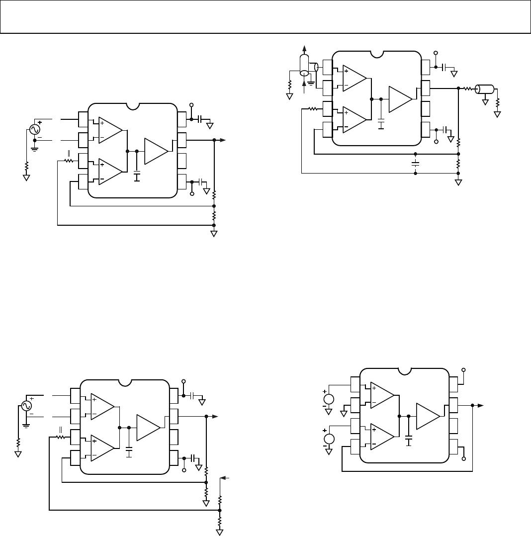
Figure 40. Gain of G Differential Amplifier, G>1
Offsetting the Output With Gain
Some applications, such as ADCs, require that the signal be
amplified and also offset, typically to accommodate the input
range of the device. The AD830 can offset the output signal
very simply through Pin 3 even with gain > 1. The voltage
applied to Pin 3 must be attenuated by an appropriate factor so
that V
3
× G = desired offset. In Figure 41, a resistive divider
from a voltage reference is used to produce the attenuated offset
voltage.
V
P
V
OUT
V
N
AD830
1
2
3
4
8
7
6
5
A = 1
G
M
G
M
C
0.1µF
0.1µF
INPUT
SIGNAL
V
CM
Z
CM
V
1
V
2
R
1
R
2
R
2
R
1
R
3
R
4
V
3
V
REF
V
OUT
= (V
1
– V
2
)(1 + R
1
/R
2
)
0
0881-041
Figure 41. Offsetting the Output with Differential Gain >1
Loop Through or Line Bridging Amplifier (Figure 42)
The AD830 is ideally suited for use as a video line bridging
amplifier. The video signal is tapped from the conductor of the
cable relative to its shield. The high input impedance of the
AD830 provides negligible loading on the cable. More significantly,
the benign loading is maintained while the AD830 is powered
down. Coupled with its good video load driving performance,
the AD830 is well suited for video cable monitoring applications.
V
P
V
OUT
V
N
AD830
1
2
3
4
8
7
6
5
A = 1
G
M
C
G
M
R
G
249
OPTIONAL C
C
499
499
75
75
0.1µF
0.1µF
0
0881-042
Figure 42. Cable Tap Amplifier
Resistorless Summing
Direct, two input, resistorless summing is easily realized from
the general unity gain mode. By grounding V
X2
and applying the
two inputs to V
X1
and V
Y1
, the output is the exact sum of the
applied voltages, V
1
and V
3
, relative to common; V
OUT
= V
1
+ V
3
.
A diagram of this simple but potent application is shown below
in Figure 43. The AD830 summing circuit possesses several
virtues not present in the classic op amp based summing circuits.
It has high impedance inputs, no resistors, very precise summing,
high reverse isolation, and noninverting gain. Achieving this
function and performance with op amps requires significantly
more components.
V
P
OUT
V
N
AD830
1
2
3
4
8
7
6
5
A = 1
G
M
C
G
M
V
1
V
3
V
OUT
= V
1
+V
3
0
0881-043
Figure 43. Resistorless Summing Amplifier
2× Gain Bandwidth Line Driver
A gain of two, without the use of resistors, is possible with the
AD830. This is accomplished by grounding V
X2
, tying the V
X1
and V
Y1
inputs together, and applying the input, V
IN
, to this
wired connection. The output is exactly twice the applied
voltage, V
IN
; V
OUT
= 2 × V
IN
. Figure 44 shows the connections
for this highly useful application. The most notable characteristic of
this alternative gain of +2 is that there is no loss of bandwidth as
in a voltage feedback op amp based gain of +2 where the
bandwidth is halved; therefore, the gain bandwidth is doubled.
In addition, this circuit is accurate without the need for any
precise valued resistors, as in the op amp equivalents, and it
possesses excellent differential gain and phase performance, as
shown in Figure 45 and Figure 46.
AD830
Rev. C | Page 17 of 20
75
75
V
P
V
OUT
V
N
AD830
1
2
3
4
8
7
6
5
A = 1
G
M
G
M
C
0.1µF
0.1µF
V
IN
00881-044
Figure 44. Full Bandwidth Line Driver (G = +2)
SUPPLYVOLTAGE (±V)
0.05
0.01
515
DIFFERENTIAL GAIN (%)
121731
0.04
0.06
0.07
0.09
4
GAIN
PHASE
GAIN = +2
R
L
= 150
FREQ = 3.58MHz
0 TO 0.7V
1110986
0.02
0.03
0.10
0.08
DIFFERENTIAL PHASE (Degrees)
0.16
0.04
0.06
0.14
0.18
0.02
0.12
0.10
0.08
0.20
0
0881-045
FREQUENCY (Hz)
0.2
10k
AMPLITUDE RESPONSE (dB)
–0.8
100k 1M 10M
100M
–0.7
–0.6
–0.5
–0.4
–0.3
–0.2
–0.1
0
0.1
V
S
= ±15V
R
L
= 150
GAIN = +2
V
S
= ±10V
V
S
= ±5V
0
0881-046
Figure 46. 0.1 dB Gain Flatness for the Circuit of Figure 44
AC-COUPLED LINE RECEIVER
The AD830 is configurable as an ac-coupled differential
amplifier on a single- or bipolar-supply voltage. All that is
needed is inclusion of a few noncritical passive components, as
illustrated in Figure 47. A simple resistive network at the X G
M
input establishes a common-mode bias. Here, the common
mode is centered at 6 V, but in principle can be any voltage
within the common-mode limits of the AD830. The 10 k
resistors to each input bias the X G
M
stage with sufficiently high
impedance to keep the input coupling corner frequency low, but
not too large so that residual bias current induced offset voltage
becomes troublesome. For dual-supply operation, the 10 k
resistors may go directly to ground. The output common is
conveniently set by a Zener diode for a low impedance
reference to preserve the high frequency CMR. However, a
simple resistive divider works fine, and good high frequency
CMR can be maintained by placing a compensating resistor in
series with the +Y input. The excellent CMRR response of the
circuit is shown in Figure 48. A plot of the 0.1 dB flatness from
10 Hz is also shown. With the use of 10 F capacitors, the CMR
is >90 dB down to a few tens of hertz. This level of performance
is almost impossible to achieve with discrete solutions.
Figure 45. Differential Gain and Phase for the Circuit of Figure 44
75
75
+12
V
OUT
1000µF
10µF
10µF
AD830
1
2
3
4
8
7
6
5
A = 1
G
M
G
M
C
0.1µF
Z
CM
75
COAX
CABLE
+12V
4.7k
6.8V
1N4736
INPUT
SIGNAL
R
T
10k
10k
2k*
+V
S
10k
10k
*OPTIONAL TUNING FOR IMPROVING
VERY LOW FREQUENCY CMR.
00881-047
Figure 47. AC-Coupled Line Receiver

AD830ARZ-REEL7

Mfr. #:
Manufacturer:
Analog Devices Inc.
Description:
Differential Amplifiers HI SPEED VIDEO
Lifecycle:
New from this manufacturer.
Delivery:
DHL FedEx Ups TNT EMS
Payment:
T/T Paypal Visa MoneyGram Western Union