Analog Input Protection
Internal protection diodes, which clamp the analog
input to V
DD
and GND, allow each input channel to
swing within (GND - 300mV) to (V
DD
+ 300mV) without
damage. However, for accurate conversions near full
scale, neither input should exceed (V
DD
+ 50mV) or be
less than (GND - 50mV).
If an off-channel analog input voltage exceeds the sup-
plies by more than 50mV, limit the forward-bias input
current to 4mA.
Track/Hold
The MAX1060/MAX1064 T/H stage enters its tracking
mode on the rising edge of WR. In external acquisition
mode, the part enters its hold mode on the next rising
edge of WR. In internal acquisition mode, the part enters
its hold mode on the fourth falling edge of the clock after
writing the control byte. Note that, in internal clock mode,
this is approximately 1µs after writing the control byte.
In single-ended operation, IN- is connected to COM
and the converter samples the positive (+) input. In
pseudo-differential operation, IN- connects to the nega-
tive input (-) and the difference of
|
(IN+) - (IN-)
|
is sam-
pled. At the beginning of the next conversion, the
positive input connects back to IN+ and C
HOLD
charges to the input signal.
The time required for the T/H stage to acquire an input
signal depends on how quickly its input capacitance is
charged. If the input signal’s source impedance is high,
the acquisition time lengthens and more time must be
allowed between conversions. The acquisition time,
t
ACQ
, is the maximum time the device takes to acquire
the signal and is also the minimum time required for the
signal to be acquired. Calculate this with the following
equation:
t
ACQ
= 7(R
S
+ R
IN
)C
IN
where R
S
is the source impedance of the input signal,
R
IN
(800) is the input resistance, and C
IN
(12pF) is
the input capacitance of the ADC. Source impedances
below 3k have no significant impact on the MAX1060/
MAX1064s’ AC performance.
Higher source impedances can be used if a 0.01µF
capacitor is connected to the individual analog inputs.
Along with the input impedance, this capacitor forms
an RC filter, limiting the ADC’s signal bandwidth.
Input Bandwidth
The MAX1060/MAX1064 T/H stage offers a 350kHz full-
linear and a 6MHz full-power bandwidth. These fea-
tures make it possible to digitize high-speed transients
and measure periodic signals with bandwidths exceed-
ing the ADC’s sampling rate by using undersampling
techniques. To avoid aliasing high-frequency signals
into the frequency band of interest, anti-alias filtering is
recommended.
Starting a Conversion
Initiate a conversion by writing a control byte that
selects the multiplexer channel and configures the
MAX1060/MAX1064 for either unipolar or bipolar opera-
tion. A write pulse (WR + CS) can either start an acqui-
sition interval or initiate a combined acquisition plus
conversion. The sampling interval occurs at the end of
MAX1060/MAX1064
400ksps, +5V, 8-/4-Channel, 10-Bit ADCs
with +2.5V Reference and Parallel Interface
10 ______________________________________________________________________________________
CH0
CH2
CH1
CH3
CH4
CH6
CH7
CH5
COM
C
SWITCH
TRACK
T/H
SWITCH
R
IN
800
C
HOLD
HOLD
10-BIT CAPACITIVE DAC
REF
ZERO
COMPARATOR
+
12pF
SINGLE-ENDED MODE: IN+ = CH0CH7, IN- = COM
PSEUDO-DIFFERENTIAL MODE: IN+ AND IN- SELECTED FROM PAIRS CH0/CH1,
CH2/CH3, CH4/CH5, AND CH6/CH7
AT THE SAMPLING INSTANT,
THE MUX INPUT SWITCHES
FROM THE SELECTED IN+
CHANNEL TO THE SELECTED
IN- CHANNEL.
INPUT
MUX
Figure 3a. MAX1060 Simplified Input Structure
CH0
CH1
CH2
CH3
COM
C
SWITCH
TRACK
T/H
SWITCH
R
IN
800
C
HOLD
HOLD
10-BIT CAPACITIVE DAC
REF
ZERO
COMPARATOR
+
12pF
SINGLE-ENDED MODE: IN+ = CH0CH3, IN- = COM
PSEUDO-DIFFERENTIAL MODE: IN+ AND IN- SELECTED FROM PAIRS CH0/CH1
AND CH2/CH3
AT THE SAMPLING INSTANT,
THE MUX INPUT SWITCHES
FROM THE SELECTED IN+
CHANNEL TO THE SELECTED
IN- CHANNEL.
INPUT
MUX
Figure 3b. MAX1064 Simplified Input Structure
MAX1060/MAX1064
400ksps, +5V, 8-/4-Channel, 10-Bit ADCs
with +2.5V Reference and Parallel Interface
______________________________________________________________________________________ 11
Table 1. Control Byte Functional Description
NAME FUNCTION
D4
0
SGL/DIF
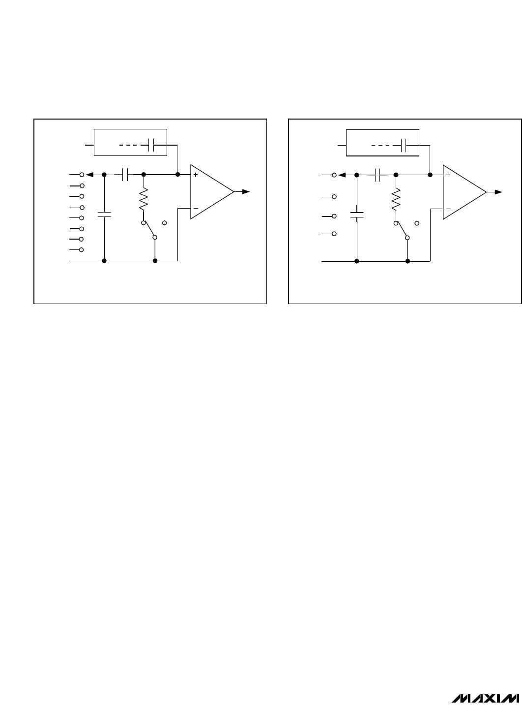
SGL/DIF = 0: Pseudo-differential analog input mode
SGL/DIF = 1: Single-ended analog input mode
In single-ended mode, input signals are referred to COM. In pseudo-differential mode, the voltage
difference between two channels is measured (Tables 2 and 3).
10
D3
UNI/BIP
Standby power-down mode. Clock mode is unaffected.
0
11
UNI/BIP = 0: Bipolar mode
UNI/BIP = 1: Unipolar mode
In unipolar mode, an analog input signal from 0 to V
REF
can be converted; in bipolar mode, the
signal can range from -V
REF
/2 to +V
REF
/2.
D2, D1, D0
Normal operation mode. External clock mode is selected.
1
A2, A1, A0
Address bits A2, A1, A0 select which of the 8/4 (MAX1060/MAX1064) channels are to be converted
(Tables 3 and 4).
Normal operation mode. Internal clock mode is selected.
BIT
PD1, PD0
0
D7, D6
PD1 and PD0 select the various clock and power-down modes.
Full power-down mode. Clock mode is unaffected.
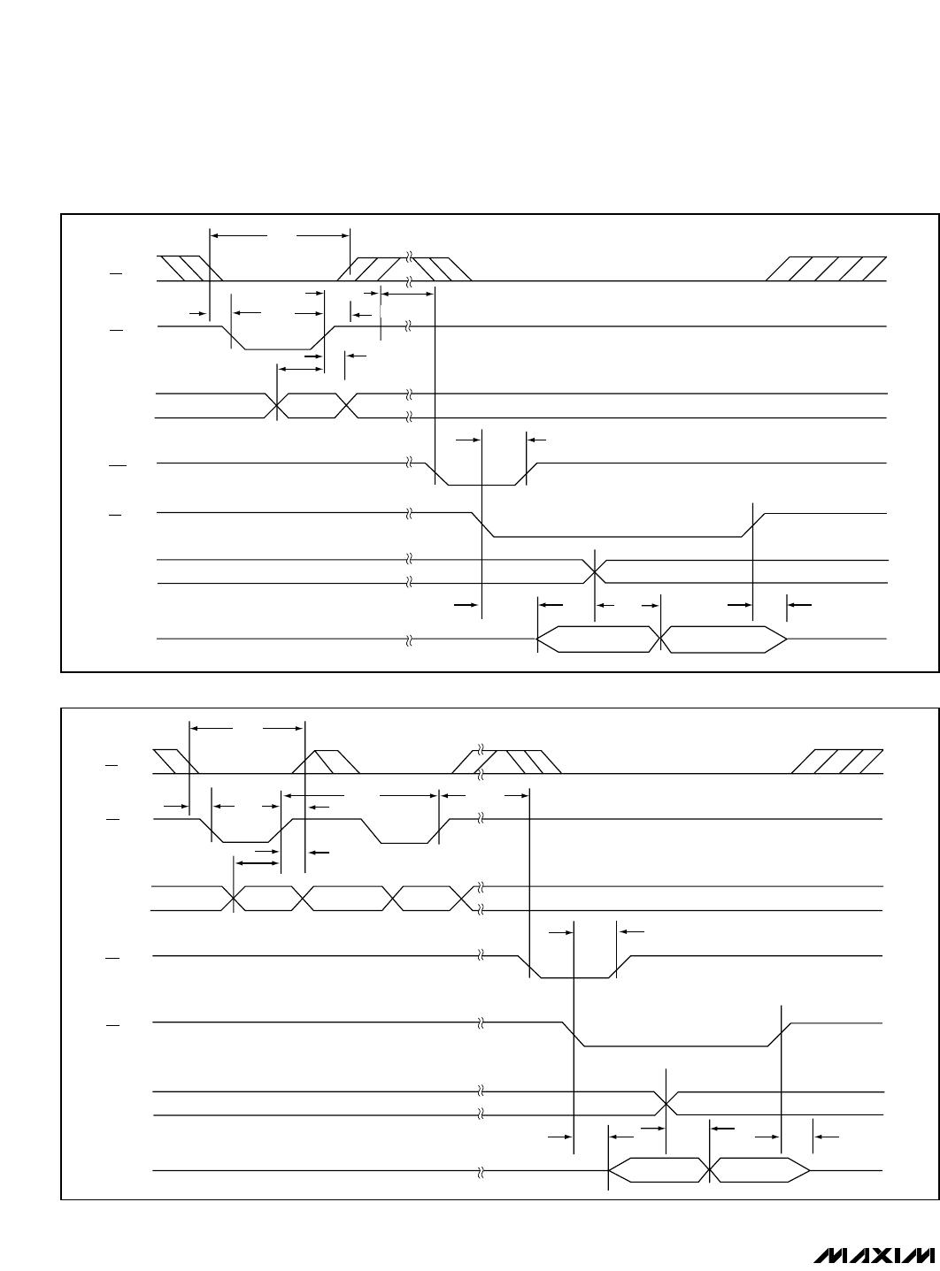
D5 ACQMOD
ACQMOD = 0: Internal acquisition mode
ACQMOD = 1: External acquisition mode
the acquisition interval. The ACQMOD (acquisition
mode) bit in the input control byte (Table 1) offers two
options for acquiring the signal: an internal and an
external acquisition. The conversion period lasts for 13
clock cycles in either the internal or external clock or
acquisition mode. Writing a new control byte during a
conversion cycle aborts the conversion and starts a
new acquisition interval.
Internal Acquisition
Select internal acquisition by writing the control byte
with the ACQMOD bit cleared (ACQMOD = 0). This
causes the write pulse to initiate an acquisition interval
whose duration is internally timed. Conversion starts
when this acquisition interval (three external clock
cycles or approximately 1µs in internal clock mode)
ends (Figure 4). When the internal acquisition is com-
bined with the internal clock, the aperture jitter can be
as high as 200ps. Internal clock users wishing to
achieve the 50ps jitter specification should always use
external acquisition mode.
External Acquisition
Use external acquisition mode for precise control of the
sampling aperture and/or dependent control of acquisi-
tion and conversion times. The user controls acquisition
and start-of-conversion with two separate write pulses.
The first pulse, written with ACQMOD = 1, starts an
acquisition interval of indeterminate length. The second
write pulse, written with ACQMOD = 0 (all other bits in
the control byte are unchanged), terminates acquisition
and starts conversion on WR rising edge (Figure 5).
The address bits for the input multiplexer must have the
same values on the first and second write pulses.
Power-down mode bits (PD0, PD1) can assume new
values on the second write pulse (see the Power-Down
Modes section). Changing other bits in the control byte
corrupts the conversion.
Reading a Conversion
A standard interrupt signal, INT, is provided to allow the
MAX1060/MAX1064 to flag the µP when the conversion
has ended and a valid result is available. INT goes low
when the conversion is complete and the output data is
ready (Figures 4 and 5). INT returns high on the first
read cycle or if a new control byte is written.
Selecting Clock Mode
The MAX1060/MAX1064 operate with an internal or
external clock. Control bits D6 and D7 select either
internal or external clock mode. The part retains the
last-requested clock mode if a power-down mode is
selected in the current input word. For both internal and
external clock modes, internal or external acquisition
can be used. At power-up, the MAX1060/MAX1064
enter the default external clock mode.
MAX1060/MAX1064
400ksps, +5V, 8-/4-Channel, 10-Bit ADCs
with +2.5V Reference and Parallel Interface
12 ______________________________________________________________________________________
t
CS
t
CSWS
t
WR
t
ACQ
t
CONV
t
DH
t
DS
t
INT1
t
D0
t
D01
t
TR
HIGH-ZHIGH-Z
CS
WR
D7D0
INT
RD
HBEN
DOUT
ACQMOD = 0
HIGH/LOW
BYTE VALID
HIGH/LOW
BYTE VALID
CONTROL
BYTE
t
CSWH
Figure 4. Conversion Timing Using Internal Acquisition Mode
t
CS
t
CSWS
t
WR
t
ACQ
t
CONV
t
DH
t
DS
t
INT1
t
D0
t
D01
t
TR
t
CSHW
ACQMOD = 1
CS
WR
D7D0
INT
RD
HBEN
DOUT
ACQMOD = 0
HIGH/LOW
BYTE VALID
HIGH/LOW
BYTE VALID
CONTROL
BYTE
CONTROL
BYTE
HIGH-Z HIGH-Z
Figure 5. Conversion Timing Using External Acquisition Mode

MAX1060AEEI+

Mfr. #:
Manufacturer:
Maxim Integrated
Description:
Analog to Digital Converters - ADC 5V 10Bit 8Ch 400ksps w/2.5V Ref & Prl Int
Lifecycle:
New from this manufacturer.
Delivery:
DHL FedEx Ups TNT EMS
Payment:
T/T Paypal Visa MoneyGram Western Union