MAX1060/MAX1064
400ksps, +5V, 8-/4-Channel, 10-Bit ADCs
with +2.5V Reference and Parallel Interface
8 _______________________________________________________________________________________
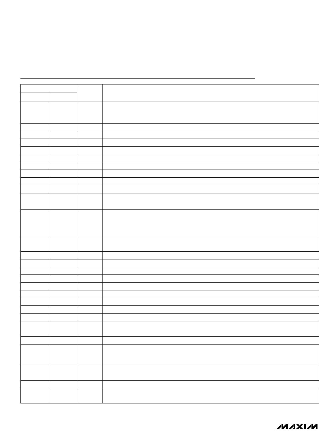
Pin Description
NAME FUNCTION
1 HBEN
High Byte Enable. Used to multiplex the 10-bit conversion result.
1: 2 MSBs are multiplexed on the data bus.
0: 8 LSBs are available on the data bus.
PIN
2 D7 Tri-State Digital I/O Line (D7)
3 D6 Tri-State Digital I/O Line (D6)
4 D5 Tri-State Digital I/O Line (D5)
5 D4 Tri-State Digital I/O Line (D4)
6 D3 Tri-State Digital I/O Line (D3)
7 D2 Tri-State Digital I/O Line (D2)
8 D1/D9 Tri-State Digital I/O Line (D1, HBEN = 0; D9, HBEN = 1)
9 D0/D8 Tri-State Digital I/O Line (D0, HBEN = 0; D8, HBEN = 1)
10
INT INT goes low when the conversion is complete and the output data is ready.
11
RD
Active-Low Read Select. If CS is low, a falling edge on RD enables the read operation on the
data bus.
12
WR
Active-Low Write Select. When CS is low in internal acquisition mode, a rising edge on WR
latches in configuration data and starts an acquisition plus a conversion cycle. When CS is
low in external acquisition mode, the first rising edge on WR ends acquisition and starts a
conversion.
13 CLK
Clock Input. In external clock mode, drive CLK with a TTL-/CMOS-compatible clock. In inter-
nal clock mode, connect this pin to either V
DD
or GND.
14
CS Active-Low Chip Select. When CS is high, digital outputs (D7–D0) are high impedance.
15 CH7 Analog Input Channel 7
16 CH6 Analog Input Channel 6
17 CH5 Analog Input Channel 5
18 CH4 Analog Input Channel 4
19 CH3 Analog Input Channel 3
20 CH2 Analog Input Channel 2
21 CH1 Analog Input Channel 1
22 CH0 Analog Input Channel 0
23 COM
Ground Reference for Analog Inputs. Sets zero-code voltage in single-ended mode and
must be stable to ±0.5 LSB during conversion.
24 GND Analog and Digital Ground
25 REFADJ
Bandgap Reference Output/Bandgap Reference Buffer Input. Bypass to GND with a 0.01µF
capacitor. When using an external reference, connect REFADJ to V
DD
to disable the internal
bandgap reference.
26 REF
Bandgap Reference Buffer Output/External Reference Input. Add a 4.7µF capacitor to GND
when using the internal reference.
27 V
DD
Analog +5V Power Supply. Bypass with a 0.1µF capacitor to GND.
28 V
LOGIC
Digital Power Supply. V
LOGIC
powers the digital outputs of the data converter and can range
from +2.7V to (V
DD
+ 300mV).
1
2
3
4
5
6
7
8
9
10
11
12
13
14
—
—
—
—
15
16
17
18
19
20
21
22
23
24
MAX1060 MAX1064