Operating mode,
MAX1060/MAX1064
400ksps, +5V, 8-/4-Channel, 10-Bit ADCs
with +2.5V Reference and Parallel Interface
4 _______________________________________________________________________________________
TIMING CHARACTERISTICS
(V
DD
= V
LOGIC
= +5V ±10%, COM = GND, REFADJ = V
DD
, V
REF
= +2.5V, 4.7µF capacitor at REF pin, f
CLK
= 7.6MHz (50% duty
cycle), T
A
= T
MIN
to T
MAX
, unless otherwise noted. Typical values are at T
A
= +25°C.)
CONDITIONS UNITSMIN TYP MAXSYMBOLPARAMETER
Standby mode
Operating mode,
f
SAMPLE
= 400ksps
1.0 1.2
mA
2.5 2.9
2.9 3.4
I
DD
Positive Supply Current
V
4.5 5.5
V
DD
Analog Supply Voltage
200
ELECTRICAL CHARACTERISTICS (continued)
(V
DD
= V
LOGIC
= +5V ±10%, COM = GND, REFADJ = V
DD
, V
REF
= +2.5V, 4.7µF capacitor at REF pin, f
CLK
= 7.6MHz (50% duty
cycle), T
A
= T
MIN
to T
MAX
, unless otherwise noted. Typical values are at T
A
= +25°C.)
V
LOGIC
Current I
LOGIC
C
L
= 20pF
210
µA
Power-Supply Rejection PSR V
DD
= 5V ±10%, full-scale input
±0.3 ±0.9
mV
f
SAMPLE
= 400ksps
Nonconverting
V
2.7
V
DD
+
0.3
V
LOGIC
Digital Supply Voltage
WR to CLK Fall Setup Time
t
CWS
40
ns
nsCLK Pulse Width High
nsCLK Period
t
CH
40
t
CP
132
CLK Pulse Width Low t
CL
40
ns
Data Valid to WR Rise Time
t
DS
40
ns
WR Rise to Data Valid Hold Time
t
DH
0
ns
CLK Fall to WR Hold Time
t
CWH
40
ns
CS to CLK or WR Setup Time
t
CSWS
60
ns
CLK or WR to CS Hold Time
t
CSWH
0
ns
CS Pulse Width
t
CS
100
ns
WR Pulse Width
t
WR
60
ns(Note 8)
PARAMETER SYMBOL MIN TYP MAX UNITSCONDITIONS
Shutdown mode
210
0.5 0.8
POWER REQUIREMENTS
µA
External reference
Internal reference
External reference
Internal reference
MAX1060/MAX1064
400ksps, +5V, 8-/4-Channel, 10-Bit ADCs
with +2.5V Reference and Parallel Interface
_______________________________________________________________________________________ 5
Note 1: Tested at V
DD
= +5V, COM = GND, unipolar single-ended input mode.
Note 2: Relative accuracy is the deviation of the analog value at any code from its theoretical value after offset and gain errors have
been removed.
Note 3: Offset nulled.
Note 4: On channel is grounded; sine wave applied to off channels.
Note 5: Conversion time is defined as the number of clock cycles times the clock period; clock has 50% duty cycle.
Note 6: Input voltage range referenced to negative input. The absolute range for the analog inputs is from GND to V
DD
.
Note 7: External load should not change during conversion for specified accuracy.
Note 8: When bit 5 is set low for internal acquisition, WR must not return low until after the first falling clock edge of the conversion.
TIMING CHARACTERISTICS (continued)
(V
DD
= V
LOGIC
= +5V ±10%, COM = GND, REFADJ = V
DD
, V
REF
= +2.5V, 4.7µF capacitor at REF pin, f
CLK
= 7.6MHz (50% duty
cycle), T
A
= T
MIN
to T
MAX
, unless otherwise noted. Typical values are at T
A
= +25°C.)
3k
3k
DOUT
DOUT
V
LOGIC
a) HIGH-Z TO V
OH
AND V
OL
TO V
OH
b) HIGH-Z TO V
OL
AND V
OH
TO V
OL
C
LOAD
20pF
C
LOAD
20pF
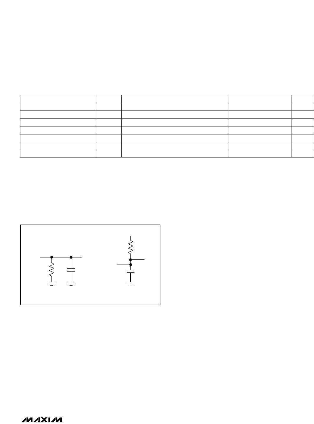
Figure 1. Load Circuits for Enable/Disable Times
t
TR
10 40
nsC
LOAD
= 20pF, Figure 1
RD Rise to Output Disable
RD Fall to Output Data Valid
t
DO
10 50
ns
RD Fall to INT High Delay
t
INT1
50
ns
CS Fall to Output Data Valid
t
DO2
100
ns
C
LOAD
= 20pF, Figure 1
C
LOAD
= 20pF, Figure 1
C
LOAD
= 20pF, Figure 1
t
TC
10 60
nsC
LOAD
= 20pF, Figure 1
PARAMETER SYMBOL MIN TYP MAX UNITSCONDITIONS
CS Rise to Output Disable
HBEN Rise to Output Data Valid t
DO1
10 50
nsC
LOAD
= 20pF, Figure 1
HBEN Fall to Output Data Valid t
DO1
10 80
nsC
LOAD
= 20pF, Figure 1
MAX1060/MAX1064
400ksps, +5V, 8-/4-Channel, 10-Bit ADCs
with +2.5V Reference and Parallel Interface
6 _______________________________________________________________________________________
Typical Operating Characteristics
(V
DD
= V
LOGIC
= +5V, V
REF
= +2.500V, f
CLK
= 7.6MHz, C
L
= 20pF, T
A
= +25°C, unless otherwise noted.)
-0.25
-0.10
-0.15
-0.20
-0.05
0
0.05
0.10
0.15
0.20
0.25
0 400200 600 800 1000 1200
INTEGRAL NONLINEARITY
vs. OUTPUT CODE
MAX1060/64 toc01
OUTPUT CODE
INL (LSB)
0.1 10k101 100 1k 100k 1M
SUPPLY CURRENT
vs. SAMPLE FREQUENCY
MAX1060/64 toc03
f
SAMPLE
(Hz)
I
DD
(µA)
1
10
100
1k
10k
WITH INTERNAL
REFERENCE
WITH EXTERNAL
REFERENCE
1.8
1.9
2.0
2.1
2.2
SUPPLY CURRENT vs. SUPPLY VOLTAGE
MAX1060/64 toc04
V
DD
(V)
I
DD
(mA)
4.50 5.004.75 5.25 5.50
R
L
=
CODE = 1010100000
1.7
1.9
1.8
2.1
2.0
2.2
2.3
-40 10-15 35 60 85
SUPPLY CURRENT vs. TEMPERATURE
MAX1060/64 toc05
TEMPERATURE (°C)
I
DD
(mA)
R
L
=
CODE = 1010100000
930
950
940
970
960
980
990
4.50 5.004.75 5.25 5.50
STANDBY CURRENT vs. SUPPLY VOLTAGE
MAX1060/64 toc06
V
DD
(V)
STANDBY I
DD
(µA)
1.0
1.5
2.0
2.5
3.0
POWER-DOWN CURRENT
vs. SUPPLY VOLTAGE
MAX1060/64 toc08
V
DD
(V)
POWER-DOWN I
DD
(µA)
4.50 5.004.75 5.25 5.50
1.8
2.0
1.9
2.1
2.2
-40 10-15 35 60 85
POWER-DOWN CURRENT
vs. TEMPERATURE
MAX1060/64 toc09
TEMPERATURE (°C)
POWER-DOWN I
DD
(µA)
-0.25
-0.10
-0.15
-0.20
-0.05
0
0.05
0.10
0.15
0.20
0.25
0 400200 600 800 1000 1200
DIFFERENTIAL NONLINEARITY
vs. OUTPUT CODE
MAX1060/64 toc02
OUTPUT CODE
DNL (LSB)

MAX1060AEEI+

Mfr. #:
Manufacturer:
Maxim Integrated
Description:
Analog to Digital Converters - ADC 5V 10Bit 8Ch 400ksps w/2.5V Ref & Prl Int
Lifecycle:
New from this manufacturer.
Delivery:
DHL FedEx Ups TNT EMS
Payment:
T/T Paypal Visa MoneyGram Western Union