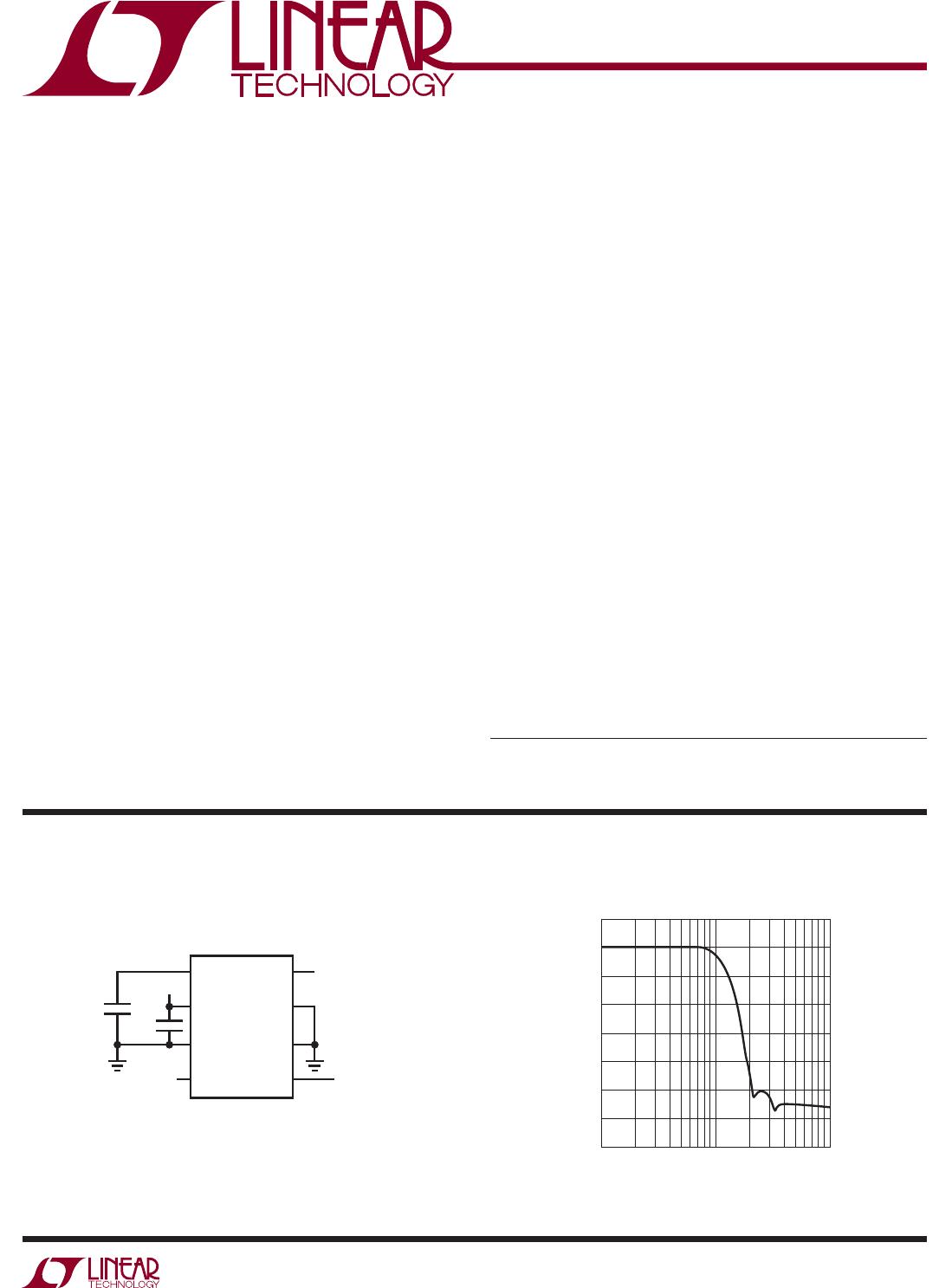
LTC1069-7IS8#TRPBF

LTC1069-7
1
10697fa
TYPICAL APPLICATION
DESCRIPTION
Linear Phase
8th Order Lowpass Filter
The LTC
®
1069-7 is a monolithic, clock-tunable, linear
phase, 8th order lowpass fi lter. The amplitude response
of the fi lter approximates a raised cosine fi lter with an
alpha of one. The gain at the cutoff frequency is –3dB and
the attenuation at twice the cutoff frequency is 43dB. The
Single 5V Supply, Linear Phase 100kHz Lowpass Filter
L, LT, LTC and LTM are registered trademarks of Linear Technology Corporation.
FEATURES
APPLICATIONS
n
8th Order, Linear Phase Filter in SO-8 Package
n
Raised Cosine Amplitude Response
n
43dB Attenuation at 2× f
CUTOFF
n
Wideband Noise: 140μV
RMS
n
Operates from Single 5V Supply to
±5V Power Supplies
n
Clock-Tunable to 200kHz with ±5V Supplies
n
Clock-Tunable to 120kHz with Single 5V Supply
n
Digital Communication Filter
n
Antialiasing Filter with Linear Phase
n
Smoothing Filters
AGND
V
+
NC
V
IN
V
IN
V
OUT
V
OUT
V
NC
CLK
LTC1069-7
f
CLK
= 2.5MHz
5V
0.47μF
0.1μF
1069-7 TA01
FREQUENCY (kHz)
10
–70
GAIN (dB)
–60
–50
–40
–30
10
100 1000
1069-7 TA02
–20
–10
0
cutoff frequency of the LTC1069-7 is set by an external
clock and is equal to the clock frequency divided by 25.
The ratio of the internal sampling frequency to the cutoff
frequency is 50:1 that is, the input signal is sampled
twice per clock cycle to lower the risk of aliasing. The
LTC1069-7 can be operated from a single 5V supply up
to dual ±5V supplies.
The gain and phase response of the LTC1069-7 can be
used in digital communication systems where pulse
shaping and channel bandwidth limiting must be carried
out. Any system that requires an analog fi lter with linear
phase and sharper roll off than conventional Bessel fi lters
can use the LTC1069-7.
The LTC1069-7 has a wide dynamic range. With ±5V
supplies and an input range of 0.1V
RMS
to 2V
RMS
, the
signal-to-(noise + THD) ratio is ≥ 60dB. The wideband noise
of the LTC1069-7 is 140μV
RMS
. Unlike other LTC1069-X fi lters,
the typical passband gain of the LTC1069-7 is equal to –1V/V.
The LTC1069-7 is available in an SO-8 package.
Other fi lter responses with lower power/speed specifi cations
can be obtained. Please contact LTC Marketing.
Frequency Response
LTC1069-7
2
10697fa
PIN CONFIGURATION ABSOLUTE MAXIMUM RATINGS
Total Supply Voltage (V
+
to V
) ............................... 12V
Power Dissipation .............................................. 400mW
Operating Temperature Range
LTC1069-7C ............................................ 0°C to 70°C
LTC1069-7I .........................................40°C to 85°C
Storage Temperature ..............................65°C to 150°C
Lead Temperature (Soldering, 10 sec) .................. 300°C
1
2
3
4
8
7
6
5
TOP VIEW
V
OUT
V
NC
CLK
AGND
V
+
NC
V
IN
S8 PACKAGE
8-LEAD PLASTIC SO
T
JMAX
= 125°C, θ
JA
= 130°C/W
ELECTRICAL CHARACTERISTICS
SYMBOL CONDITIONS MIN TYP MAX UNITS
Passband Gain (f
IN
≤ 0.2f
CUTOFF
)V
S
= ±5V, f
CLK
= 2.5MHz
f
TEST
= 1kHz, V
IN
= 1V
RMS
l
0.10 ±0.75
±0.90
dB
dB
V
S
= 4.75V, f
CLK
= 500kHz
f
TEST
= 1kHz, V
IN
= 0.5V
RMS
l
0.10 ±0.75
±0.90
dB
dB
Gain at 0.25f
CUTOFF
V
S
= ±5V, f
CLK
= 2.5MHz
f
TEST
= 25kHz, V
IN
= 1V
RMS
l
–0.55
–0.30
0.1
dB
dB
V
S
= 4.75V, f
CLK
= 500kHz
f
TEST
= 5kHz, V
IN
= 0.5V
RMS
l
–0.30
–0.05
0.15
dB
dB
Gain at 0.50f
CUTOFF
V
S
= ±5V, f
CLK
= 2.5MHz
f
TEST
= 50kHz, V
IN
= 1V
RMS
l –1.40
1.0
–0.35
dB
dB
V
S
= 4.75V, f
CLK
= 500kHz
f
TEST
= 10kHz, V
IN
= 0.5V
RMS
l –0.60
–0.30
0
dB
dB
Gain at 0.75f
CUTOFF
V
S
= ±5V, f
CLK
= 2.5MHz
f
TEST
= 75kHz, V
IN
= 1V
RMS
l 2.1
–1.65
–0.80
dB
dB
V
S
= 4.75V, f
CLK
= 500kHz
f
TEST
= 15kHz, V
IN
= 0.5V
RMS
l –1.15
–0.75
–0.25
dB
dB
Gain at f
CUTOFF
V
S
= ±5V, f
CLK
= 2.5MHz
f
TEST
= 100kHz, V
IN
= 1V
RMS
l 4.0
3.5
2.7
dB
dB
V
S
= 4.75V, f
CLK
= 500kHz
f
TEST
= 20kHz, V
IN
= 0.5V
RMS
l 3.3
2.9
2.4
dB
dB
The l denotes specifi cations which apply over the full operating
temperature range. f
CUTOFF
is the fi lters cutoff frequency and is equal to f
CLK
/25. The f
CLK
signal level is TTL or CMOS (max clock rise
or fall time ≤1μs), R
L
= 10k, T
A
= 25°C, unless otherwise specifi ed. All AC gains are measured relative to the passband gain.
ORDER INFORMATION
LEAD FREE FINISH TAPE AND REEL PART MARKING PACKAGE DESCRIPTION TEMPERATURE RANGE
LTC1069-7CS8#PBF LTC1069-7CS8#TRPBF 10697 8-Lead Plastic SO 0°C to 70°C
LTC1069-7IS8#PBF LTC1069-7IS8#TRPBF 10697I 8-Lead Plastic SO 40°C to 85°C
Consult LTC Marketing for parts specifi ed with wider operating temperature ranges.
Consult LTC Marketing for information on non-standard lead based fi nish parts.
For more information on lead free part marking, go to: http://www.linear.com/leadfree/
For more information on tape and reel specifi
cations, go to: http://www.linear.com/tapeandreel/
LTC1069-7
3
10697fa
Note 1: Stresses beyond those listed under Absolute Maximum Ratings
may cause permanent damage to the device. Exposure to any Absolute
Maximum Rating condition for extended periods may affect device
reliability and lifetime.
Note 2: Phase Deviation = 1/2(Phase at 0Hz – Phase at f
CUTOFF
) – (Phase
at 0Hz – Phase at 0.5f
CUTOFF
)
Phase at 0Hz = 180° (guaranteed by design)
ELECTRICAL CHARACTERISTICS
The l denotes specifi cations which apply over the full operating
temperature range.
f
CUTOFF
is the fi lters cutoff frequency and is equal to f
CLK
/25. The f
CLK
signal level is TTL or CMOS (max clock rise
or fall time ≤1μs), R
L
= 10k, T
A
= 25°C, unless otherwise specifi ed. All AC gains are measured relative to the passband gain.
SYMBOL CONDITIONS MIN TYP MAX UNITS
Gain at 1.5f
CUTOFF
V
S
= ±5V, f
CLK
= 2.5MHz
f
TEST
= 150kHz, V
IN
= 1V
RMS
–19
–16.5
–14
dB
dB
V
S
= 4.75V, f
CLK
= 500kHz
f
TEST
= 30kHz, V
IN
= 0.5V
RMS
–20
–18.1
–17
dB
dB
Gain at 2.0f
CUTOFF
V
S
= ±5V, f
CLK
= 2.5MHz
f
TEST
= 200kHz, V
IN
= 1V
RMS
–55
–43
–38
dB
dB
V
S
= 4.75V, f
CLK
= 500kHz
f
TEST
= 40kHz, V
IN
= 0.5V
RMS
–48
–41
–39
dB
dB
Gain at 5.0f
CUTOFF
V
S
= 4.75V, f
CLK
= 500kHz
f
TEST
= 100kHz, V
IN
= 0.5V
RMS
70 59 55 dB
Gain at f
CUTOFF
(160kHz) V
S
= ±5V, f
CLK
= 4MHz
f
TEST
= 160kHz, V
IN
= 1V
RMS
2.1 dB
Phase at 0.5f
CUTOFF
V
S
= ±5V, f
CLK
= 2.5MHz
f
TEST
= 50kHz
35 30.5 25 Deg
Phase at f
CUTOFF
V
S
= ±5V, f
CLK
= 2.5MHz
f
TEST
= 100kHz
240 235 230 Deg
Passband Phase Deviation from
Linear Phase (Note 1)
V
S
= ±5V, f
CLK
= 500kHz 3.0 Deg
Output DC Offset (Input at GND) V
S
= ±5V, f
CLK
= 500kHz
V
S
= 4.75V, f
CLK
= 400kHz
50
25
125
mV
mV
Output Voltage Swing V
S
= ±5V, I
SOURCE
/I
SINK
≤ 1mA, R
L
= 10k
V
S
= 4.75V, I
SOURCE
/I
SINK
≤ 1mA, R
L
= 10k
l
l
±3.5
2.6
±4.0
3.6
V
V
P-P
Power Supply Current V
S
= ±5V, f
CLK
= 500kHz
l
18 26
29
mA
mA
V
S
= 4.75V, f
CLK
= 400kHz
l
13 15
16.5
mA
mA
Example: An LTC1069-7 has Phase at 0.5f
CUTOFF
= –30.5° and Phase at
f
CUTOFF
= –235°.
Passband Phase Deviation from Linear Phase
= 1/2[180° – (–235°)] – [(180° – (–30.5°)] = –

LTC1069-7IS8#TRPBF

Mfr. #:
Manufacturer:
Analog Devices Inc.
Description:
Active Filter Linear Phase 8th Order Lowpass Filter
Lifecycle:
New from this manufacturer.
Delivery:
DHL FedEx Ups TNT EMS
Payment:
T/T Paypal Visa MoneyGram Western Union