LTC1069-7
7
10697fa
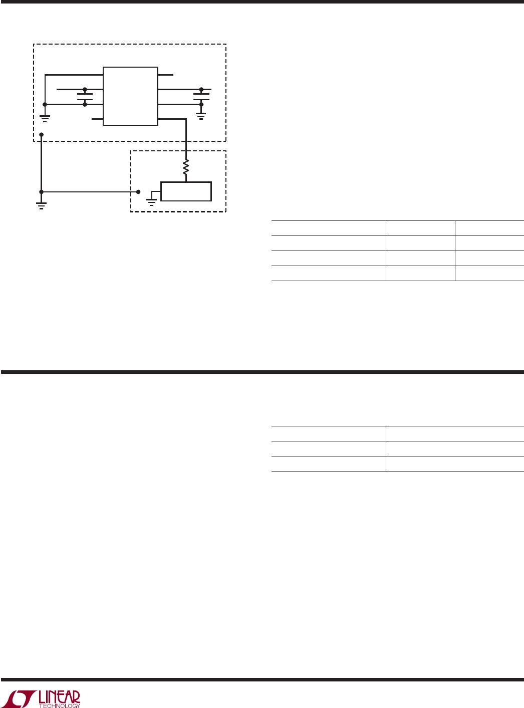
CLK (Pin 5): Clock Input. Any TTL or CMOS clock source
with a square wave output and 50% duty cycle (±10%) is
an adequate clock source for the device. The power supply
for the clock source should not necessarily be the fi lter’s
power supply. The analog ground of the fi lter should only
be connected to the clock’s ground at a single point. Table
1 shows the clock’s low and high level threshold value for
V
–
1069 F02
1k
V
+
LTC1069-7
CLOCK
SOURCE
0.1μF
ANALOG GROUND
PLANE
8
7
6
5
AGND
V
+
NC
V
IN
1
2
3
4
V
OUT
V
–
NC
CLK
STAR
SYSTEM
GROUND
DIGITAL
GROUND
PLANE
V
IN
0.1μF
V
OUT
Figure 2. Connections for Dual Supply Operation
PIN FUNCTIONS
a dual or single supply operation. A pulse generator can
be used as a clock source provided the high level on-time
is greater than 0.42μs (V
S
= ± 5V). Sine waves less than
100kHz are not recommended for clock sources because
excessive slow clock rise or fall times generate internal
clock jitter. The maximum clock rise or fall time is 1μs. The
clock signal should be routed from the right side of the IC
package to avoid coupling into any input or output analog
signal path. A 1k resistor between the clock source and the
clock input (Pin 5) will slow down the rise and fall times
of the clock to further reduce charge coupling, Figure 1.
Table 1. Clock Source High and Low Thresholds
POWER SUPPLY HIGH LEVEL LOW LEVEL
Dual Supply = ±5V 1.5V 0.5V
Single Supply = 10V 6.5V 5.5V
Single Supply = 5V 1.5V 0.5V
V
OUT
(Pin 8): Filter Output. Pin 8 is the output of the fi lter,
and it can source 23mA or sink 16mA. The total harmonic
distortion of the fi lter will degrade when driving coaxial
cables or loads less than 20k without an output buffer.
APPLICATIONS INFORMATION
Temperature Behavior
The power supply current of the LTC1069-7 has a positive
temperature coeffi cient. The GBW product of its internal
op amps is nearly constant and the speed of the device
does not degrade at high temperatures.
Clock Feedthrough
The clock feedthrough is defi ned as the RMS value of the
clock frequency and its harmonics that are present at the
fi lter’s output (Pin 8). The clock feedthrough is tested with
the input (Pin 4) shorted to the AGND pin and depends on
PC board layout and on the value of the power supplies.
With proper layout techniques the values of the clock
feedthrough are shown on Table 2.
Table 2. Clock Feedthrough
V
S
CLOCK FEEDTHROUGH
5V 400μV
RMS
±5V 850μV
RMS
Any parasitic switching transients during the rising and
falling edges of the incoming clock are not part of the
clock feedthrough specifi cations. Switching transients
have frequency contents much higher than the applied
clock; their amplitude strongly depends on scope probing
techniques as well as grounding and power supply
bypassing. The clock feedthrough can be reduced by
adding a single RC lowpass fi lter at the output (Pin 8) of
the LTC1069-7.