_______________General Description
The dual MAX492, quad MAX494, and single MAX495
operational amplifiers combine excellent DC accuracy
with rail-to-rail operation at the input and output. Since
the common-mode voltage extends from V
CC
to V
EE
,
the devices can operate from either a single supply
(+2.7V to +6V) or split supplies (±1.35V to ±3V). Each
op amp requires less than 150µA supply current. Even
with this low current, the op amps are capable of driving
a 1kΩ load, and the input referred voltage noise is only
25nV/√Hz. In addition, these op amps can drive loads in
excess of 1nF.
The precision performance of the MAX492/MAX494/
MAX495, combined with their wide input and output
dynamic range, low-voltage single-supply operation, and
very low supply current, makes them an ideal choice for
battery-operated equipment and other low-voltage appli-
cations. The MAX492/MAX494/MAX495 are available in
DIP and SO packages in the industry-standard op-amp
pin configurations. The MAX495 is also available in the
smallest 8-pin SO: the µMAX package.
________________________Applications
Portable Equipment
Battery-Powered Instruments
Data Acquisition
Signal Conditioning
Low-Voltage Applications
____________________________Features
♦ Low-Voltage Single-Supply Operation (+2.7V to +6V)
♦ Rail-to-Rail Input Common-Mode Voltage Range
♦ Rail-to-Rail Output Swing
♦ 500kHz Gain-Bandwidth Product
♦ Unity-Gain Stable
♦ 150µA Max Quiescent Current per Op Amp
♦ No Phase Reversal for Overdriven Inputs
♦ 200µV Offset Voltage
♦ High Voltage Gain (108dB)
♦ High CMRR (90dB) and PSRR (110dB)
♦ Drives 1kΩ Load
♦ Drives Large Capacitive Loads
♦ MAX495 Available in µMAX Package—8-Pin SO
______________Ordering Information
Ordering Information continued at end of data sheet.
*
Dice are specified at TA = +25°C, DC parameters only.
MAX492/MAX494/MAX495
Single/Dual/Quad, Micropower,
Single-Supply Rail-to-Rail Op Amps
________________________________________________________________
Maxim Integrated Products
1
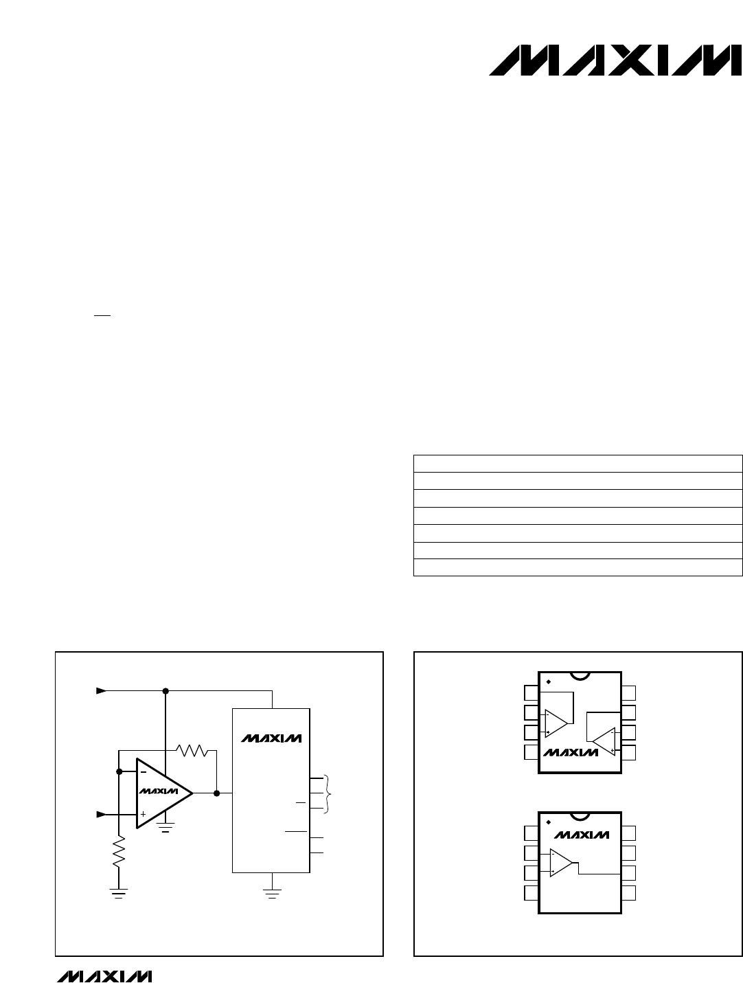
1
2
3
4
8
7
6
5
V
CC
OUT2
IN2-
IN2+
V
EE
IN1+
IN1-
OUT1
MAX492
DIP/SO
TOP VIEW
1
2
3
4
8
7
6
5
N.C.
V
CC
OUT
NULL
V
EE
IN1+
IN1-
NULL
MAX495
DIP/SO/µMAX
_________________Pin Configurations
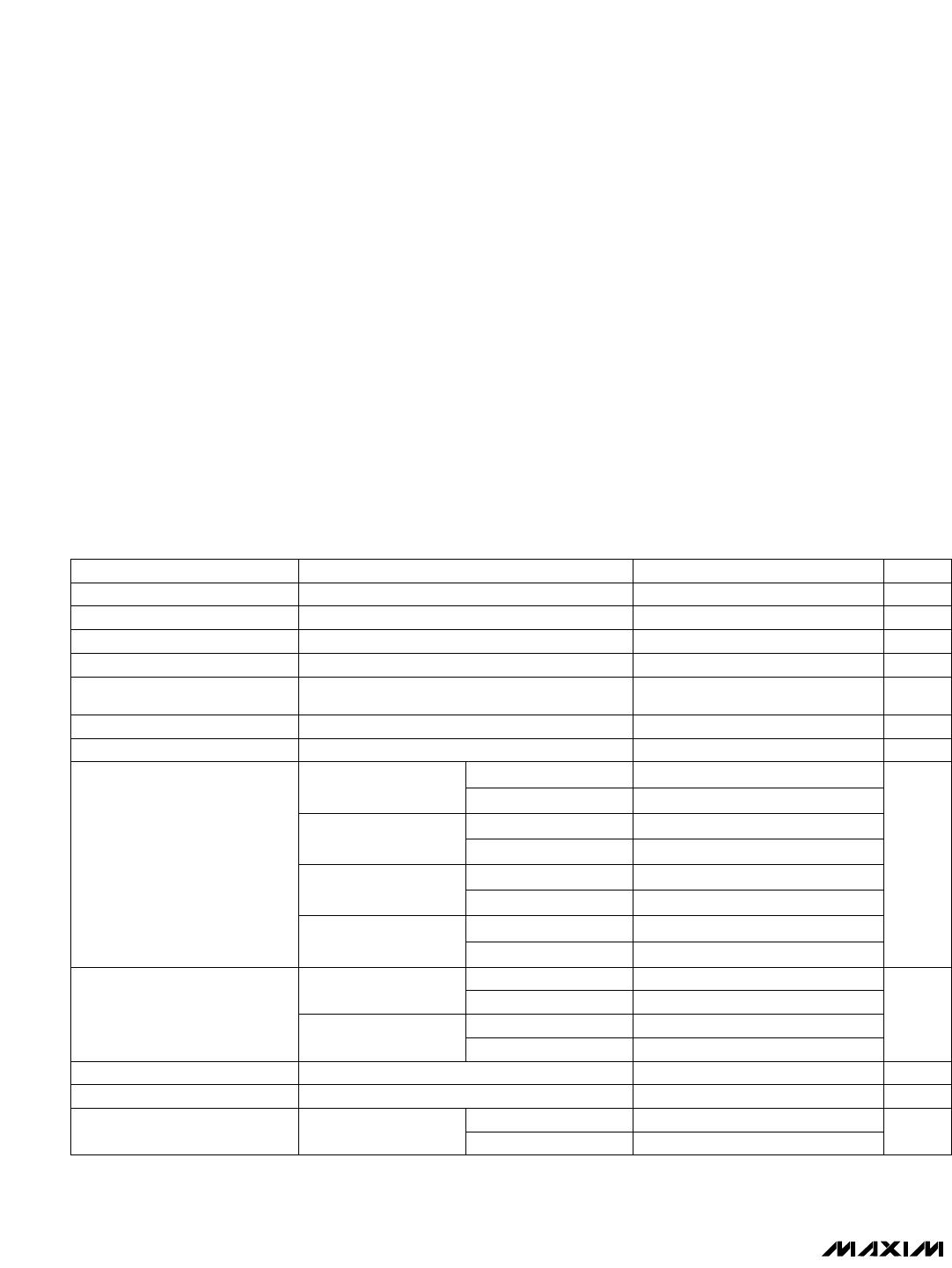
MAX187
(ADC)
GND
INPUT SIGNAL CONDITIONING FOR LOW-VOLTAGE ADC
V
DD
SERIAL
INTERFACE
6
8
7
3
1
4.096V
4
AIN
5
DOUT
SCLK
CS
SHDN
REF
2
ANALOG
INPUT
+5V
6
7
4
2
3
10k
10k
MAX495
__________Typical Operating Circuit
For free samples & the latest literature: http://www.maxim-ic.com, or phone 1-800-998-8800
19-0265; Rev 2; 9/96
PART
MAX492CPA
MAX492CSA
MAX492C/D 0°C to +70°C
0°C to +70°C
0°C to +70°C
TEMP. RANGE PIN-PACKAGE
8 Plastic DIP
8 SO
Dice*
MAX492EPA
MAX492ESA -40°C to +85°C
-40°C to +85°C 8 Plastic DIP
8 SO
MAX492MJA -55°C to +125°C 8 CERDIP
Pin Configurations continued at end of data sheet.