MAX492/MAX494/MAX495
Single/Dual/Quad, Micropower,
Single-Supply Rail-to-Rail Op Amps
_______________________________________________________________________________________ 9
____________________________Typical Operating Characteristics (continued)
(T
A
= +25°C, V
CC
= 5V, V
EE
= 0V, unless otherwise noted.)
V
IN
2V/div
V
OUT
2V/div
V
CC
= +5V, A
V
= -1, R
L
= 10k
50µs/div
LARGE-SIGNAL TRANSIENT RESPONSE
V
IN
2V/div
V
OUT
2V/div
V
CC
= +5V, A
V
= +1, R
L
= 10k
50µs/div
LARGE-SIGNAL TRANSIENT RESPONSE
______________________________________________________________Pin Description
Amplifier OutputOUT
Amplifier 2 Inverting InputIN2-6
Amplifier 2 OutputOUT27
Positive Power-Supply Pin. Connect to (+) terminal of power supply.V
CC
8
Amplifier 3 OutputOUT3
Noninverting InputIN+
Amplifier 1 Noninverting InputIN1+3
Negative Power-Supply Pin. Connect to ground or a negative voltage.V
EE
4
Amplifier 2 Noninverting InputIN2+5
Amplifier 1 Inverting InputIN1-2
Inverting InputIN-
Offset Null Input. Connect to a 10kpotentiometer for offset-voltage trimming.
Connect wiper to V
EE
(Figure 3).
NULL
Amplifier 1 OutputOUT11
FUNCTION
MAX492
NAME
6
7
4
8
3
11
5
2
1
MAX494
6
7
3
4
2
PIN
1, 5
MAX495
Amplifier 3 Inverting InputIN3-
Amplifier 3 Noninverting InputIN3+
Amplifier 4 Noninverting InputIN4+
9
10
12
Amplifier 4 Inverting InputIN4-
Amplifier 4 OutputOUT4
No Connect. Not internally connected.N.C.
13
14
8
MAX492/MAX494/MAX495
Single/Dual/Quad, Micropower,
Single-Supply Rail-to-Rail Op Amps
10 ______________________________________________________________________________________
MAX495
10k
1
5
NULL
V
EE
4
NULL
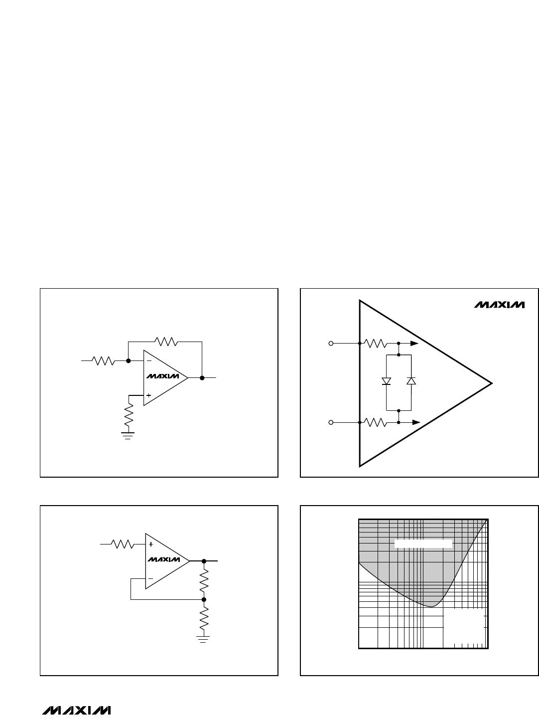
Figure 2. Offset Null Circuit
__________Applications Information
The dual MAX492, quad MAX494, and single MAX495
op amps combine excellent DC accuracy with rail-to-
rail operation at both input and output. With their preci-
sion performance, wide dynamic range at low supply
voltages, and very low supply current, these op amps
are ideal for battery-operated equipment and other low-
voltage applications.
Rail-to-Rail Inputs and Outputs
The MAX492/MAX494/MAX495’s input common-mode
range extends 0.25V beyond the positive and negative
supply rails, with excellent common-mode rejection.
Beyond the specified common-mode range, the out-
puts are guaranteed not to undergo phase reversal or
latchup. Therefore, the MAX492/MAX494/MAX495 can
be used in applications with common-mode signals at
or even beyond the supplies, without the problems
associated with typical op amps.
The MAX492/MAX494/MAX495’s output voltage swings
to within 50mV of the supplies with a 100k load. This
rail-to-rail swing at the input and output substantially
increases the dynamic range, especially in low supply-
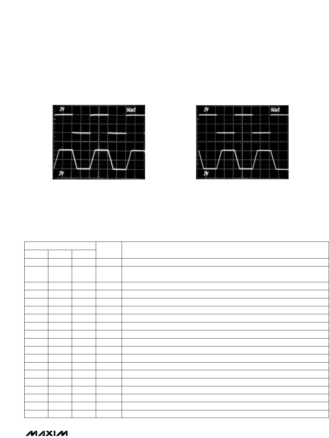
voltage applications. Figure 1 shows the input and out-
put waveforms for the MAX492, configured as a
unity-gain noninverting buffer operating from a single
+3V supply. The input signal is 3.0V
p-p
, 1kHz sinusoid
centered at +1.5V. The output amplitude is approxi-
mately 2.95V
p-p
.
Input Offset Voltage
Rail-to-rail common-mode swing at the input is obtained
by two complementary input stages in parallel, which
feed a folded cascaded stage. The PNP stage is active
for input voltages close to the negative rail, and the
NPN stage is active for input voltages close to the posi-
tive rail.
The offsets of the two pairs are trimmed; however, there
is some small residual mismatch between them. This
mismatch results in a two-level input offset characteris-
tic, with a transition region between the levels occurring
at a common-mode voltage of approximately 1.3V.
Unlike other rail-to-rail op amps, the transition region
has been widened to approximately 600mV in order to
minimize the slight degradation in CMRR caused by
this mismatch.
To adjust the MAX495’s input offset voltage (500µV max
at +25°C), connect a 10k trim potentiometer between
the two NULL pins (pins 1 and 5), with the wiper con-
nected to V
EE
(pin 4) (Figure 2). The trim range of this
circuit is ±6mV. External offset adjustment is not avail-
able for the dual MAX492 or quad MAX494.
The input bias currents of the MAX492/MAX494/MAX495
are typically less than 50nA. The bias current flows into
the device when the NPN input stage is active, and it
flows out when the PNP input stage is active. To reduce
the offset error caused by input bias current flowing
through external source resistances, match the effec-
tive resistance seen at each input. Connect resistor R3
between the noninverting input and ground when using
V
IN
V
OUT
Figure 1. Rail-to-Rail Input and Output (Voltage Follower
Circuit, V
CC
= +3V, V
EE
= 0V)
MAX492/MAX494/MAX495
Single/Dual/Quad, Micropower,
Single-Supply Rail-to-Rail Op Amps
the op amp in an inverting configuration (Figure 3a);
connect resistor R3 between the noninverting input and
the input signal when using the op amp in a noninvert-
ing configuration (Figure 3b). Select R3 to equal the
parallel combination of R1 and R2. High source resis-
tances will degrade noise performance, due to the ther-
mal noise of the resistor and the input current noise
(which is multiplied by the source resistance).
Input Stage Protection Circuitry
The MAX492/MAX494/MAX495 include internal protec-
tion circuitry that prevents damage to the precision
input stage from large differential input voltages. This
protection circuitry consists of back-to-back diodes
between IN+ and IN- with two 1.7kresistors in series
(Figure 4). The diodes limit the differential voltage
applied to the amplifiers
internal circuitry to no more
than V
F
, where V
F
is the diodes
forward-voltage drop
(about 0.7V at +25°C).
Input bias current for the ICs (±25nA typical) is speci-
fied for the small differential input voltages. For large
differential input voltages (exceeding V
F
), this protec-
tion circuitry increases the input current at IN+ and IN-:
(V
IN
+ - V
IN
- ) - V
F
Input Current = ———————————
2 x 1.7k
For comparator applications requiring large differential
voltages (greater than V
F
), you can limit the input cur-
rent that flows through the diodes with external resistors
R1
V
OUT
R3 = R2
II
R1
R3
V
IN
R2
MAX49_
Figure 3a. Reducing Offset Error Due to Bias Current:
Inverting Configuration
R3
V
OUT
R3 = R2
II
R1
V
IN
R1
R2
MAX49_
MAX492
MAX494
MAX495
1.7k
1.7k
TO INTERNAL
CIRCUITRY
TO INTERNAL
CIRCUITRY
IN–
IN+
Figure 4. Input Stage Protection Circuitry
10,000
100
1 10 100
MAX492-FG 04
RESISTIVE LOAD (k)
CAPACITIVE LOAD (pF)
1000
UNSTABLE REGION
V
CC
= +5V
V
OUT
= V
CC
/2
R
L
TO V
EE
A
V
= +1
Figure 5. Capacitive-Load Stable Region Sourcing Current
______________________________________________________________________________________ 11
Figure 3b. Reducing Offset Error Due to Bias Current:
Noninverting Configuration

MAX494CSD-T

Mfr. #:
Manufacturer:
Maxim Integrated
Description:
Operational Amplifiers - Op Amps uPower Single-Supply Rail-Rail
Lifecycle:
New from this manufacturer.
Delivery:
DHL FedEx Ups TNT EMS
Payment:
T/T Paypal Visa MoneyGram Western Union