WM8781 Production Data
w
PD, January 2012, Rev 4.5
2
TABLE OF CONTENTS
DESCRIPTION ....................................................................................................... 1
FEATURES ............................................................................................................ 1
APPLICATIONS ..................................................................................................... 1
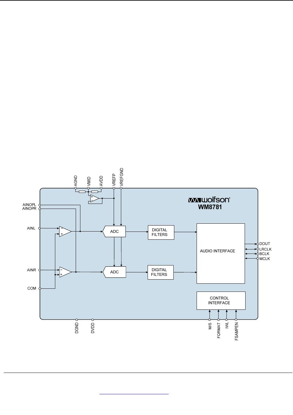
BLOCK DIAGRAM ................................................................................................ 1
TABLE OF CONTENTS ......................................................................................... 2
PIN CONFIGURATION .......................................................................................... 3
ORDERING INFORMATION .................................................................................. 3
PIN DESCRIPTION ................................................................................................ 4
ABSOLUTE MAXIMUM RATINGS ........................................................................ 5
THERMAL PERFORMANCE ................................................................................. 5
RECOMMENDED OPERATING CONDITIONS ..................................................... 5
ELECTRICAL CHARACTERISTICS ..................................................................... 6
TERMINOLOGY ............................................................................................................... 7
SIGNAL TIMING REQUIREMENTS ...................................................................... 8
DEVICE DESCRIPTION ...................................................................................... 10
INTRODUCTION ............................................................................................................ 10
ADC ................................................................................................................................ 10
ADC DIGITAL FILTER ................................................................................................... 10
DIGITAL AUDIO INTERFACE ........................................................................................ 11
POWER DOWN CONTROL ........................................................................................... 14
POWER ON RESET ...................................................................................................... 14
DIGITAL FILTER CHARACTERISTICS .............................................................. 16
ADC FILTER RESPONSES ........................................................................................... 16
ADC HIGH PASS FILTER .............................................................................................. 17
APPLICATIONS INFORMATION ........................................................................ 18
RECOMMENDED EXTERNAL COMPONENTS ............................................................ 18
RECOMMENDED EXTERNAL COMPONENTS VALUES ............................................. 18
PACKAGE DIAGRAM ......................................................................................... 19
IMPORTANT NOTICE ......................................................................................... 20
ADDRESS: ..................................................................................................................... 20