WM8781 Production Data
w
PD, January 2012, Rev 4.5
10
DEVICE DESCRIPTION
INTRODUCTION
The WM8781 is a stereo 24-bit ADC designed for demanding recording applications such as DVD
recorders, studio mixers, PVRs, and AV amplifiers. The WM8781 consists of stereo line level inputs,
followed by a sigma-delta modulator and digital filtering.
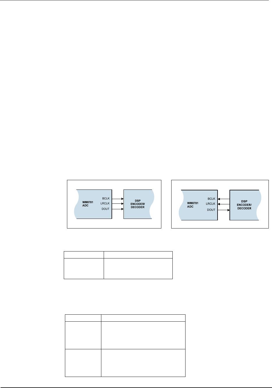
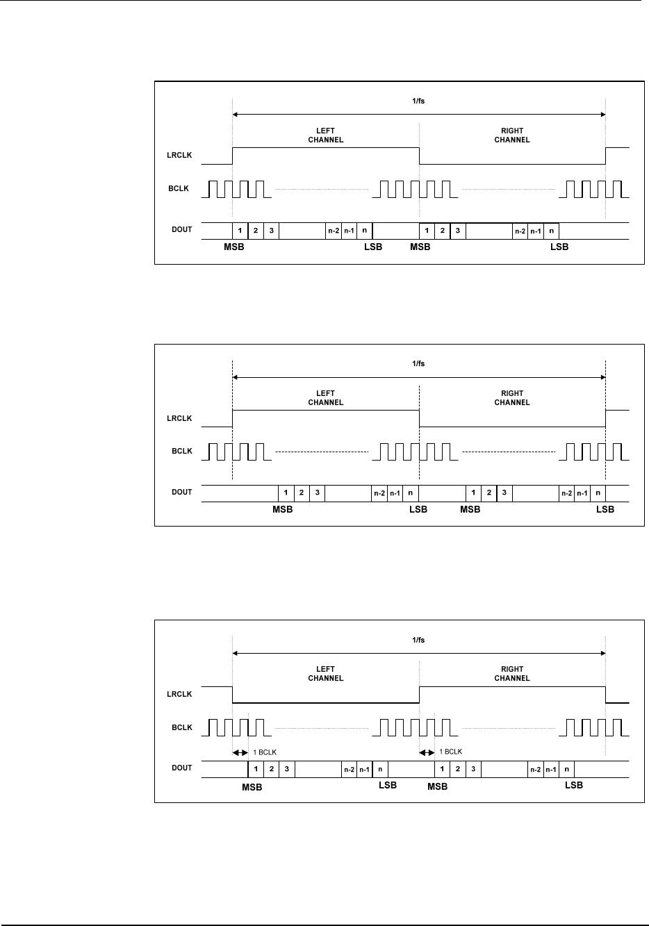
The device offers stereo line level inputs along with two control input pins (FORMAT, IWL) to allow
operation of the audio interface in three industry standard modes (left justified, right justified or I
2
S) .
An internal op-amp is integrated on the front end of the chip to accommodate analogue input signals
greater than 1V
rms
. The device also has a high pass filter to remove residual DC offsets.
The WM8781 offers Master or Slave mode clocking schemes. A control input pin M/S is used to allow
Slave mode or Master mode operation. The WM8781 supports master clock rates from 128fs to 768fs
and digital audio output word lengths from 16-24 bits. Sampling rates from 8kHz to 192kHz are
supported, delivering high SNR operating with 128x, 64x or 32x over-sampling, according to the
sample rate.
The line inputs are biased internally through the operational amplifier to V
MID
.
ADC
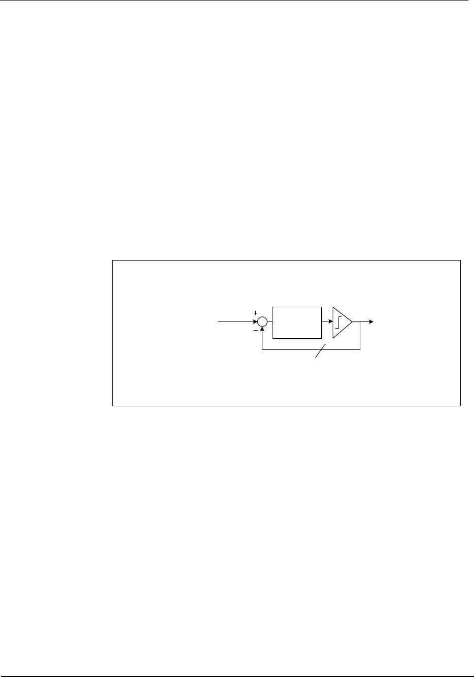
The WM8781 uses a multi-bit over sampled sigma-delta ADC. A single channel of the ADC is
illustrated in Figure 4 Multi-Bit Oversampling Sigma Delta ADC Schematic.
LIN/RIN
ANALOG
INTEGRATOR
MULTI
BITS
TO ADC DIGITAL FILTERS
Figure 4 Multi-Bit Oversampling Sigma Delta ADC Schematic
The use of multi-bit feedback and high oversampling rates reduces the effects of jitter and high
frequency noise.
The ADC Full Scale input is 1.0V rms at AVDD = 5.0 volts. Any input voltage greater than full scale
will possibly overload the ADC and cause distortion. Note that the full scale input has a linear
relationship with AVDD. The internal op-amp and appropriate resistors can be used to reduce signals
greater than 1Vrms before they reach the ADC.
The ADC filters perform true 24 bit signal processing to convert the raw multi-bit oversampled data
from the ADC to the correct sampling frequency to be output on the digital audio interface.
ADC DIGITAL FILTER
The ADC digital filters contain a digital high pass filter. The high-pass filter response detailed in Digital
Filter Characteristics. The operation of the high pass filter removes residual DC offsets that are
present on the audio signal.
Production Data WM8781
w
PD, January 2012, Rev 4.5
11
DIGITAL AUDIO INTERFACE
The digital audio interface uses three pins:
DOUT: ADC data output
LRCLK: ADC data alignment clock
BCLK: Bit clock, for synchronisation
The digital audio interface takes the data from the internal ADC digital filters and places it on DOUT
and LRCLK. DOUT is the formatted digital audio data stream output from the ADC digital filters with
left and right channels multiplexed together. LRCLK is an alignment clock that controls whether Left
or Right channel data is present on the DOUT line. DOUT and LRCLK are synchronous with the
BCLK signal with each data bit transition signified by a BCLK high to low transition. DOUT is always
an output. BCLK and LRCLK maybe an inputs or outputs depending whether the device is in Master
or Slave mode. (see Master and Slave Mode Operation, below).
Three different audio data formats are supported:
Left justified
Right justified
I
2
S
MASTER AND SLAVE MODE OPERATION
The WM8781 can be configured as either a master or slave mode device. As a master device the
WM8781 generates BCLK and LRCLK and thus controls sequencing of the data transfer on DOUT. In
slave mode, the WM8781 responds with data to clocks it receives over the digital audio interface. The
mode can be selected by setting the MS input pin (see Table 4 Master/Slave selection below).
Master and slave modes are illustrated below.
Figure 5 Master Mode Figure 6 Slave Mode
PIN DESCRIPTION
M/S Master/Slave Selection
0 = Slave Mode
1= Master Mode
Table 4 Master/Slave selection
AUDIO INTERFACE CONTROL
The Input Word Length and Audio Format mode can be selected by using IWL and FORMAT pins.
PIN DESCRIPTION
IWL Word Length
0 = 16 bit
1 = 20 bit
Z = 24 bit
FORMAT Audio Mode Select
0 = RJ
1 = LJ
Z = I2S
Table 5 Audio Data Format Control
WM8781 Production Data
w
PD, January 2012, Rev 4.5
12
AUDIO DATA FORMATS
In Left Justified mode, the MSB is available on the first rising edge of BCLK following an LRCLK
transition. The other bits up to the LSB are then transmitted in order. Depending on word length,
BCLK frequency and sample rate, there may be unused BCLK cycles before each LRCLK transition.
Figure 7 Left Justified Audio Interface (assuming n-bit word length)
In Right Justified mode, the LSB is available on the last rising edge of BCLK before an LRCLK
transition. All other bits are transmitted before (MSB first). Depending on word length, BCLK
frequency and sample rate, there may be unused BCLK cycles after each LRCLK transition.
Figure 8 Right Justified Audio Interface (assuming n-bit word length)
In I
2
S mode, the MSB is available on the second rising edge of BCLK following an LRCLK transition.
The other bits up to the LSB are then transmitted in order. Depending on word length, BCLK
frequency and sample rate, there may be unused BCLK cycles between the LSB of one sample and
the MSB of the next.
Figure 9 I
2
S Audio Interface (assuming n-bit word length)

WM8781GEDS/V

Mfr. #:
Manufacturer:
Cirrus Logic
Description:
Audio A/D Converter ICs STEREO ADC W/384FS MASTER MODE
Lifecycle:
New from this manufacturer.
Delivery:
DHL FedEx Ups TNT EMS
Payment:
T/T Paypal Visa MoneyGram Western Union

Products related to this Datasheet