2-OUTPUT 1.8V PCIE GEN1/2/3 ZERO DELAY / FANOUT BUFFER WITH ZO=100OHMS 6 REVISION F 04/28/16
9DBV0241 DATASHEET
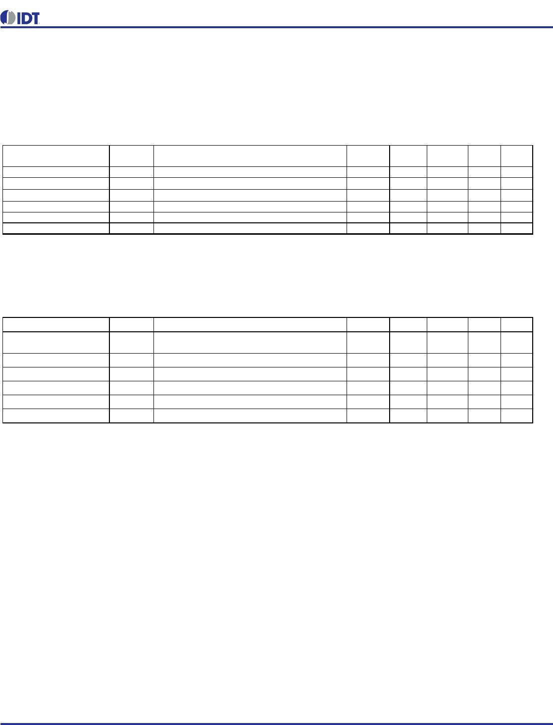
Electrical Characteristics–Input/Supply/Common Parameters–Normal Operating
Conditions
TA = T
AMB,
Supply Voltages per normal operation conditions, See Test Loads for Loading Conditions
PARAMETER SYMBOL CONDITIONS MIN TYP MAX UNITS NOTES
Supply Voltage VDDx Supply voltage for core and analog 1.7 1.8 1.9 V
Commmercial range 0 25 70 °C
Industrial range -40 25 85 °C
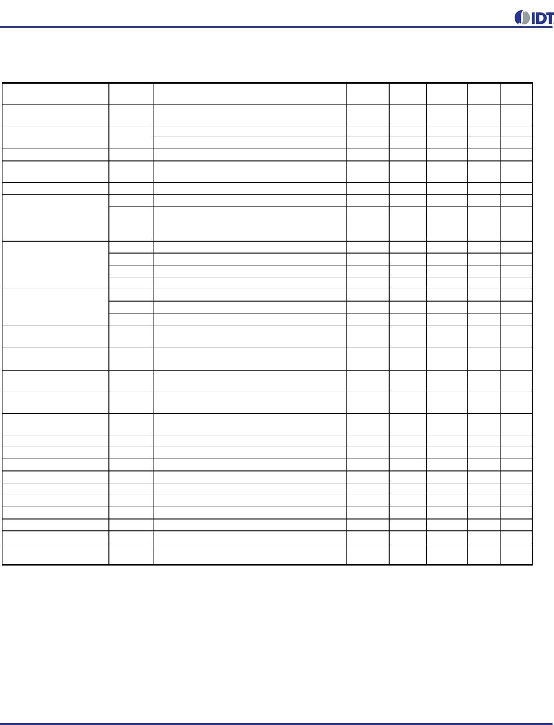
Input High Voltage V
IH
Single-ended inputs, except SMBus 0.75 V
DD
DD
+ 0.3 V
Input Mid Voltage V
IM
Single-ended tri-level inputs ('_tri' suffix) 0.4 V
DD
0.6 V
DD
V
Input Low Voltage V
IL
Single-ended inputs, except SMBus -0.3 0.25 V
DD
IN
IN
IN
= VDD -5 5 uA
I
INP
Single-ended inputs
V
IN
= 0 V; Inputs with internal pull-up resistors
V
IN
= VDD; Inputs with internal pull-down resistors
-200 200 uA
F
ib
Bypass mode 1 200 MHz 2
F
i
ll
100MHz PLL mode 60 100.00 140 MHz 2
F
i
ll
125MHz PLL mode 75 125.00 175 MHz 2
F
i
ll
50MHz PLL mode 30 50.00 65 MHz 2
C
IN
Logic Inputs, except DIF_IN 1.5 5 pF 1
C
INDIF_IN
DIF_IN differential clock inputs 1.5 2.7 pF 1,5
C
OUT
Output pin capacitance 6 pF 1
Clk Stabilization T
STAB
From V
DD
Power-Up and after input clock
stabilization or de-assertion of PD# to 1st clock
1ms1,2
Input SS Modulation
Frequency PCIe
f
MODI NPCI e
Allowable Frequency for PCIe Applications
(Triangular Modulation)
30 33 kHz
Input SS Modulation
Frequency non-PCIe
f
MODI N
Allowable Frequency for non-PCIe Applications
(Triangular Modulation)
066kHz
OE# Latency t
LATOE#
DIF start after OE# assertion
DIF stop after OE# deassertion
1 3 clocks 1,3
Tdrive_PD# t
DRVPD
DIF output enable after
PD# de-assertion
Fall time of single-ended control inputs 5 ns 2
Trise t
R
Rise time of single-ended control inputs 5 ns 2
SMBus Input Low Voltage V
ILSMB
DDSMB
DDSMB
< 3.3V 0.6 V
SMBus Input High Voltage V
IHSMB
DDSMB
DDSMB
< 3.3V 2.1 3.6 V 4
SMBus Output Low Voltage V
OLSMB
PULLUP
0.4 V
SMBus Sink Current I
PULLUP
OL
4mA
Nominal Bus Voltage V
DDSMB
Bus Voltage 1.7 3.6 V
SCLK/SDATA Rise Time t
RSMB
(Max VIL - 0.15) to (Min VIH + 0.15) 1000 ns 1
SCLK/SDATA Fall Time t
FSMB
(Min VIH + 0.15) to (Max VIL - 0.15) 300 ns 1
SMBus Operating
Frequency
f
MAXSMB
Maximum SMBus operating frequency 400 kHz 6
1
Guaranteed by design and characterization, not 100% tested in production.
2
Control input must be monotonic from 20% to 80% of input swing.
3
Time from deassertion until out
uts are >200 mV
DIF_IN input
The differential in
ut clock must be runnin
for the SMBus to be active
For V
DDSMB
< 3.3V, V
IHSMB
>= 0.8xV
DDSMB
Input Current
Input Frequency
Capacitance
Ambient Operating
Temperature
T
AMB