16
Shunt Connections
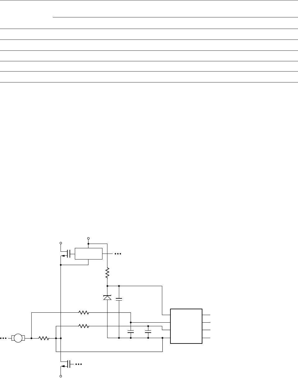
The recommended method for connecting the isolated
modulator to the shunt resistor is shown in Figure 17.
V
IN+
(pin 2 of the HPCL-7560) is connected to the posi-
tive terminal of the shunt resistor, while V
IN-
(pin 3) is
shorted to GND1 with the power-supply return path
functioning as the sense line to the negative terminal of
the current shunt. This allows a single pair of wires or PC
board traces to connect the isolated modulator circuit
to the shunt resistor. By referencing the input circuit
to the negative side of the sense resistor, any load cur-
rent induced noise transients on the shunt are seen as
a common-mode signal and will not interfere with the
current-sense signal. This is important because the large
load currents owing through the motor drive, along
with the parasitic inductances inherent in the wiring of
the circuit, can generate both noise spikes and osets
that are relatively large compared to the small voltages
that are being measured across the current shunt.
If the same power supply is used both for the gate drive
circuit and for the current sensing circuit, it is very im-
portant that the connection from GND1 of the isolated
modulator to the sense resistor be the only return path
for supply current to the gate drive power supply in
order to eliminate potential ground loop problems. The
only direct connection between the isolated modulator
circuit and the gate drive circuit should be the positive
power supply line.
resistive element itself; these two terminals are used to
monitor the voltage across the resistive element while
the other two terminals are used to carry the load cur-
rent. Because of the Kelvin connection, any voltage
drops across the leads carrying the load current should
have no impact on the measured voltage.
Several four-terminal shunts from Isotek (Isabellen-
hütte) suitable for sensing currents in motor drives up
to 71 Arms (71 hp or 53 kW) are shown in Table 3; the
maximum current and motor power range for each
of the PBV series shunts are indicated. For shunt resis-
tances from 50 mW down to 10 mW, the maximum cur-
rent is limited by the input voltage range of the isolated
modulator. For the 5 mW and 2 mW shunts, a heat sink
may be required due to the increased power dissipation
at higher currents.
When laying out a PC board for the shunts, a couple of
points should be kept in mind. The Kelvin connections
to the shunt should be brought together under the
body of the shunt and then run very close to each other
to the input of the isolated modulator; this minimizes
the loop area of the connection and reduces the pos-
sibility of stray magnetic elds from interfering with the
measured signal. If the shunt is not located on the same
PC board as the isolated modulator circuit, a tightly
twisted pair of wires can accomplish the same thing.
Also, multiple layers of the PC board can be used to
increase current carrying capacity. Numerous plated-
through vias should surround each non-Kelvin terminal
of the shunt to help distribute the current between the
layers of the PC board. The PC board should use 2 or 4
oz. copper for the layers, resulting in a current carrying
capacity in excess of 20 A. Making the current carrying
traces on the PC board fairly large can also improve the
shunt’s power dissipation capability by acting as a heat
sink. Liberal use of vias where the load current enters
and exits the PC board is also recommended.
17
Table 3. Isotek (Isabellenhütte) Four-Terminal Shunt Summary.
In some applications, however, supply currents owing
through the power-supply return path may cause oset
or noise problems. In this case, better performance may
be obtained by connecting V
IN+
and V
IN-
directly across
the shunt resistor with two conductors, and connecting
GND1 to the shunt resistor with a third conductor for
the power-supply return path, as shown in Figure 19.
When connected this way, both input pins should be
bypassed. To minimize electromagnetic interference of
the sense signal, all of the conductors (whether two or
three are used) connecting the isolated modulator to
the sense resistor should be either twisted pair wire or
closely spaced traces on a PC board.
Figure 19. Schematic for Three Conductor Shunt Connection.
Shunt
Resistor Part
Num
Shunt Resistance Tol.
Maximum RMS
Current
Motor Power Range
120 V
ac
-440 V
ac
mW % A hp kW
PBV-R050-0.5 50 0.5 3 0.8 - 3 0.6 - 2
PBV-R020-0.5 20 0.5 7 2 - 7 0.6 - 2
PBV-R010-0.5 10 0.5 14 4 - 14 3 - 10
PBV-R005-0.5 5 0.5 25 [28] 7 - 25 [8 - 28] 5 - 19 [6 - 21]
PBV-R002-0.5 2 0.5 39 [71] 11 - 39 [19 - 71] 8 - 29 [14 - 53]
The 39W resistor in series with the input lead (R2) forms
a lowpass anti-aliasing filter with the 0.01µF input
bypass capacitor (C2) with a 400 kHz bandwidth. The
resistor performs another important function as well;
it dampens any ringing which might be present in the
circuit formed by the shunt, the input bypass capacitor,
and the inductance of wires or traces connecting the
two. Undamped ringing of the input circuit near the
input sampling frequency can alias into the baseband
producing what might appear to be noise at the output
of the device.
+
-
MOTOR
HV-
HV+
R
SENSE
FLOATING
POSITIVE
SUPPLY
GATE DRIVE
CIRCUIT
V
DD1
V
IN+
V
IN-
GND1
V
DD2
MCLK
MDAT
GND2
HCPL-7560
C1
0.1 µF
C2a
0.01 µF
R2a 39
R1
D1
5.1 V
C2b
0.01 µF
R2b 39
Note: Values in brackets are with a heatsink for the shunt.
Voltage Sensing
The HCPL-7560 Isolated Modulator can also be used to
isolate signals with amplitudes larger than its recom-
mended input range with the use of a resistive voltage
divider at its input. The only restrictions are that the
impedance of the divider be relatively small (less than 1
kW) so that the input resistance (280 kW) and input bias
current (1µA) do not aect the accuracy of the mea-
surement. An input bypass capacitor is still required,
although the 39W series damping resistor is not (the
resistance of the voltage divider provides the same
function). The low-pass lter formed by the divider re-
sistance and the input bypass capacitor may limit the
achievable bandwidth. To obtain higher bandwidth,
the input bypass capacitor (C2) can be reduced, but it
should not be reduced much below 1000 pF to maintain
adequate input bypassing of the isolated modulator.
For product information and a complete list of distributors, please go to our web site: www.avagotech.com
Avago, Avago Technologies, and the A logo are trademarks of Avago Technologies, Limited in the United States and other countries.
Data subject to change. Copyright © 2006 Avago Technologies Limited. All rights reserved. Obsoletes 5989-2164EN
AV02-0408EN - June 18, 2007

HCPL-7560-500E

Mfr. #:
Manufacturer:
Broadcom / Avago
Description:
Optically Isolated Amplifiers Isolated Modulator
Lifecycle:
New from this manufacturer.
Delivery:
DHL FedEx Ups TNT EMS
Payment:
T/T Paypal Visa MoneyGram Western Union