HSMP-4820-BLKG

HSMP-382x, 482x
Surface Mount RF PIN Switch and Limiter Diodes
Data Sheet
Features
Diodes Optimized for:
Low Current Switching
Low Distortion Attenuating
Power Limiting/Circuit Protection
Surface Mount SOT-23 and SOT-323 Packages
Single and Dual Versions
Tape and Reel Options Available
Low Failure in Time (FIT) Rate
[1]
Lead-free
Note:
1. For more information see the Surface Mount PIN Reliability
Data Sheet.
Package Lead Code Identi cation, SOT-323 (Top View)
Description/Applications
The HSMP-382x series is optimized for switch ing ap-
plications where ultra-low resistance is required. The
HSMP-482x diode is ideal for limiting and low induc-
tance switching applications up to 1.5 GHz.
A SPICE model is not available for PIN diodes as SPICE
does not provide for a key PIN diode characteristic, carrier
lifetime.
Package Lead Code Identi cation, SOT-23 (Top View)
COMMON
CATHODE
#4
COMMON
ANODE
#3
SERIES
#2
SINGLE
#0
DUAL ANODE
HSMP-4820
DUAL ANODE
HSMP-482B
2
Absolute Maximum Ratings
[1]
T
C
= +25°C
Symbol Parameter Unit SOT-23 SOT-323
I
f
Forward Current (1 μs Pulse) Amp 1 1
P
IV
Peak Inverse Voltage V 50
50
T
j
Junction Temperature °C 150 150
T
stg
Storage Temperature °C -65 to 150 -65 to 150
θ
jc
Thermal Resistance
[2]
°C/W 500 150
Notes:
1. Operation in excess of any one of these conditions may result in permanent damage to the
device.
2. T
C
= +25°C, where T
C
is de ned to be the temperature at the package pins where contact is
made to the circuit board.
Minimum Maximum Typical Maximum Typical
Part Package Breakdown Series Total Total Total
Number Marking Lead Voltage Resistance Capacitance Capacitance Inductance
HSMP- Code Code Con guration V
BR
(V) R
S
(Ω) C
T
(pF) C
T
(pF) L
T
(nH)
4820 FA A Dual Anode 50 0.6 0.75 1.2 1.0
482B FA A
Dual Anode
Test Conditions V
R
= V
BR
I
F
= 10 mA f = 1 MHz f = 1 MHz f = 500 MHz
Measure V
R
= 20 V V
R
= 0 V 3 GHz
I
R
≤ 10 μA
High Frequency (Low Inductance, 500 MHz – 3 GHz) PIN Diodes
Electrical Speci cations T
C
= 25°C
Package Minimum Maximum Maximum
Part Number Marking Lead Breakdown Series Resistance Total Capacitance
HSMP- Code Code Con guration Voltage V
BR
(V) R
S
(Ω) C
T
(pF)
3820 F0 0 Single 50 0.6 0.8
3822 F2 2 Series
3823 F3 3 Common Anode
3824 F4 4 Common Cathode
Test Conditions V
R
= V
BR
f = 100 MHz f = 1 MHz
Measure I
F
= 10 mA V
R
= 20 V
I
R
≤ 10 μA
Typical Parameters at T
C
= 25°C
Part Number Series Resistance Carrier Lifetime Reverse Recovery Time Total Capacitance
HSMP- R
S
(Ω) τ (ns) T
rr
(ns) C
T
(pF)
382x 1.5 70 7 0.60 @ 20 V
Test Conditions f = 100 MHz I
F
= 10 mA V
R
= 10 V
I
F
= 10 mA I
F
= 20 mA
90% Recovery
3
Typical Parameters at T
C
= 25°C (unless otherwise noted), Single Diode
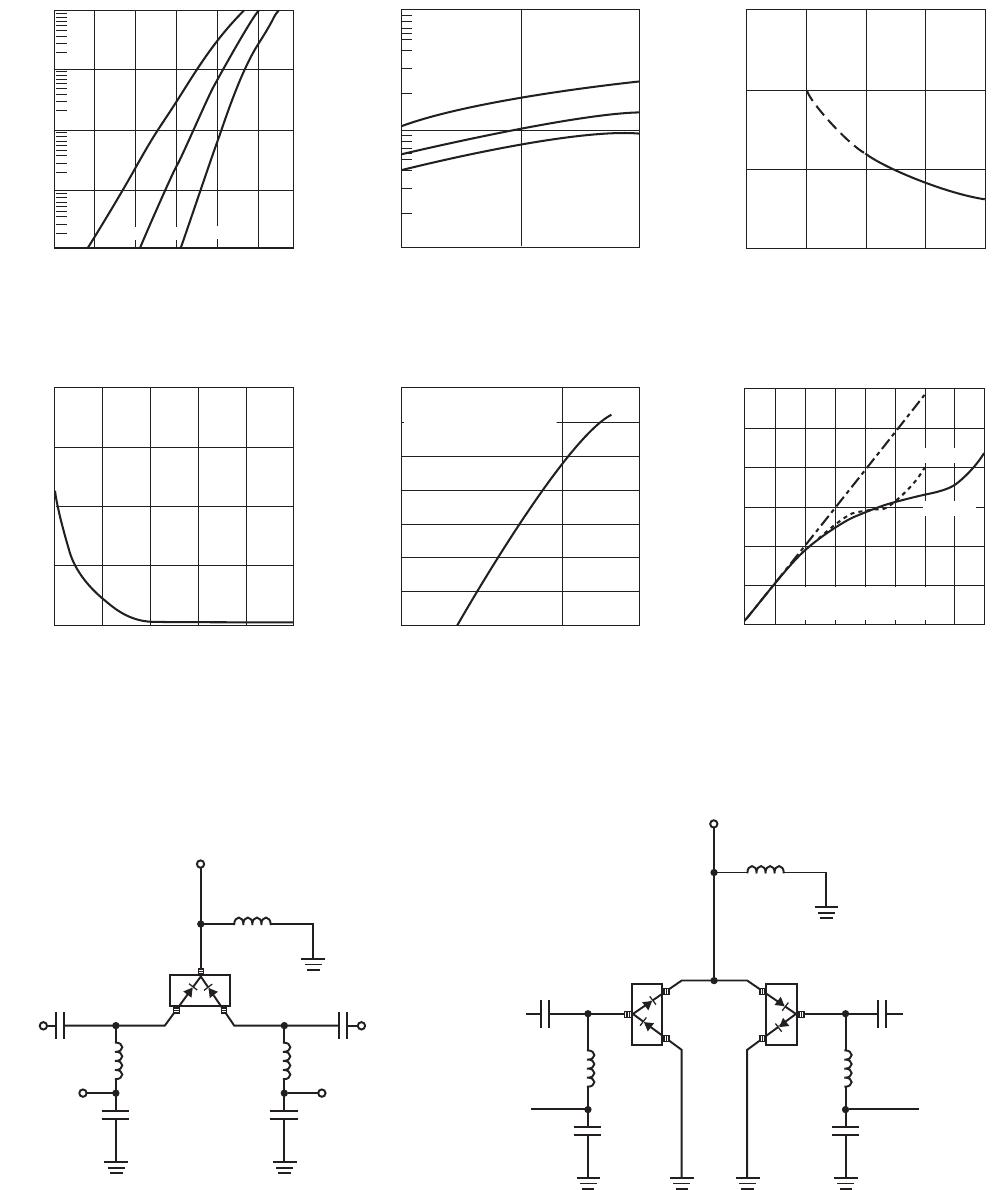
Figure 3. RF Resistance at 25C vs. Forward Bias
Current.
100
10
1
0.1
RF RESISTANCE (OHMS)
I
F
– FORWARD BIAS CURRENT (mA)
0.01 0.1 1 10 100
1.4
1.2
1.0
0.8
0.6
0 1020304050
V
R
– REVERSE VOLTAGE (V)
CAPACITANCE (pF)
Figure 4. Capacitance vs. Reverse Voltage.
120
115
110
105
100
95
90
85
11030
I
F
– FORWARD BIAS CURRENT (mA)
Figure 5. 2nd Harmonic Input Intercept Point vs.
Forward Bias Current.
INPUT INTERCEPT POINT (dBm)
Diode Mounted as a
Series Attenuator in a
50 Ohm Microstrip and
Tested at 123 MHz
FORWARD CURRENT (mA)
Figure 2. Reverse Recovery Time vs. Forward
Current for Various Reverse Voltages.
T
rr
– REVERSE RECOVERY TIME (ns)
1
10
100
10 20 30
V
R
= 2V
V
R
= 5V
V
R
= 10V
100
10
1
0.1
0.01
0 0.2 0.4 0.6 0.8 1.0 1.2
I
F
– FORWARD CURRENT (mA)
V
F
– FORWARD VOLTAGE (mA)
Figure 1. Forward Current vs. Forward Voltage.
125C
25C
–50C
CW POWER IN (dBm)
Figure 6. Large Signal Transfer Curve of the
HSMP-482x Limiter.
CW POWER OUT (dBm)
0
30
25
20
15
10
5
0
4010
5
20 25 30 3515
Measured with external
bias return
1.0 GHz
1.5 GHz
Typical Applications for Multiple Diode Products
RF COMMON
RF 1
BIAS 1
RF 2
BIAS 2
Figure 7. Simple SPDT Switch, Using Only Positive Current.
Figure 8. High Isolation SPDT Switch, Dual Bias.
RF COMMON
BIAS BIAS
RF 2
RF 1

HSMP-4820-BLKG

Mfr. #:
Manufacturer:
Broadcom / Avago
Description:
RF DIODE PIN 50V SOT23-3
Lifecycle:
New from this manufacturer.
Delivery:
DHL FedEx Ups TNT EMS
Payment:
T/T Paypal Visa MoneyGram Western Union