HSMP-4820-BLKG

7
SMT Assembly
Reliable assembly of surface mount components is a
complex process that involves many material, process,
and equipment factors, including: method of heating
(e.g., IR or vapor phase re ow, wave soldering, etc.) circuit
board material, conductor thickness and pattern, type of
solder alloy, and the thermal conductivity and thermal
mass of components. Components with a low mass, such
as the SOT-323/-23 package, will reach solder re ow
temperatures faster than those with a greater mass.
Avagos diodes have been quali ed to the time-
temperature pro le shown in Figure 21. This pro le is
representative of an IR re ow type of surface mount
assembly process.
After ramping up from room temperature, the circuit
board with components attached to it (held in place with
solder paste) passes through one or more preheat zones.
The preheat zones increase the temperature of the
board and components to prevent thermal shock and
begin evaporating solvents from the solder paste. The
re ow zone brie y elevates the temperature su ciently
to produce a re ow of the solder.
The rates of change of temperature for the ramp-up and
cool-down zones are chosen to be low enough to not
cause deformation of the board or damage to components
due to thermal shock. The maximum temperature in the
re ow zone (T
MAX
) should not exceed 260°C.
These parameters are typical for a surface mount
assembly process for Avago diodes. As a general
guideline, the circuit board and components should be
exposed only to the minimum temperatures and times
necessary to achieve a uniform re ow of solder.
Figure 21. Surface Mount Assembly Pro le.
25
Time
Temperature
Tp
T
L
tp
t
L
t 25° C to Peak
Ramp-up
ts
Ts
min
Ramp-down
Preheat
Critical Zone
T
L
to Tp
Ts
max
Lead-Free Re ow Pro le Recommendation (IPC/JEDEC J-STD-020C)
Re ow Parameter Lead-Free Assembly
Average ramp-up rate (Liquidus Temperature (T
S(max)
to Peak) 3°C/ second max
Preheat Temperature Min (T
S(min)
) 150°C
Temperature Max (T
S(max)
) 200°C
Time (min to max) (t
S
) 60-180 seconds
Ts(max) to TL Ramp-up Rate 3°C/second max
Time maintained above: Temperature (T
L
) 217°C
Time (t
L
) 60-150 seconds
Peak Temperature (T
P
) 260 +0/-5°C
Time within 5 °C of actual Peak temperature (t
P
) 20-40 seconds
Ramp-down Rate 6°C/second max
Time 25 °C to Peak Temperature 8 minutes max
Note 1: All temperatures refer to topside of the package, measured on the package body surface
8
Package Characteristics
Lead Material ....................................................... Copper (SOT-323); Alloy 42 (SOT-23)
Lead Finish ............................................................................ Tin 100% (Lead-free option)
Maximum Soldering Temperature ............................................... 260°C for 5 seconds
Minimum Lead Strength .............................................................................. 2 pounds pull
Typical Package Inductance ..........................................................................................2 nH
Typical Package Capacitance ................................................. 0.08 pF (opposite leads)
Ordering Information
Specify part number followed by option. For example:
HSMP - 382x - XXX
Bulk or Tape and Reel Option
Part Number; x = Lead Code
Surface Mount PIN
Option Descriptions
-BLKG = Bulk, 100 pcs. per antistatic bag
-TR1G = Tape and Reel, 3000 devices per 7" reel
-TR2G = Tape and Reel, 10,000 devices per 13" reel
Tape and Reeling conforms to Electronic Industries RS-481, Taping of Surface
Mounted Components for Automated Placement.
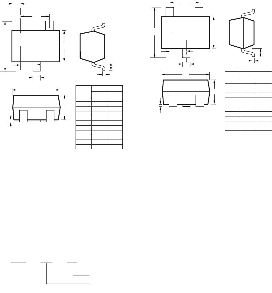
Package Dimensions
Outline 23 (SOT-23)
Outline SOT-323 (SC-70)
e
B
e2
e1
E1
C
E
XXX
L
D
A
A1
Notes:
XXX-package marking
Drawings are not to scale
DIMENSIONS (mm)
MIN.
0.79
0.000
0.30
0.08
2.73
1.15
0.89
1.78
0.45
2.10
0.45
MAX.
1.20
0.100
0.54
0.20
3.13
1.50
1.02
2.04
0.60
2.70
0.69
SYMBOL
A
A1
B
C
D
E1
e
e1
e2
E
L
e
B
e1
E1
C
E
XXX
L
D
A
A1
Notes:
XXX-package marking
Drawings are not to scale
DIMENSIONS (mm)
MIN.
0.80
0.00
0.15
0.08
1.80
1.10
1.80
0.26
MAX.
1.00
0.10
0.40
0.25
2.25
1.40
2.40
0.46
SYMBOL
A
A1
B
C
D
E1
e
e1
E
L
1.30 typical
0.65 typical
9
Tape Dimensions and Product Orientation
For Outline SOT-23
Device Orientation
For Outlines SOT-23/323
USER
FEED
DIRECTION
COVER TAPE
CARRIER
TAPE
REEL
Note: "AB" represents package marking code.
"C" represents date code.
END VIEW
8 mm
4 mm
TOP VIEW
ABC ABC ABC ABC
9 MAX
A
0
P
P
0
D
P
2
E
F
W
D
1
Ko
8 MAX
B
0
13.5 MAX
t1
DESCRIPTION SYMBOL SIZE (mm) SIZE (INCHES)
LENGTH
WIDTH
DEPTH
PITCH
BOTTOM HOLE DIAMETER
A
0
B
0
K
0
P
D
1
3.15 ± 0.10
2.77 ± 0.10
1.22
± 0.10
4.00
± 0.10
1.00 + 0.05
0.124
± 0.004
0.109
± 0.004
0.048 ± 0.004
0.157 ± 0.004
0.039 ± 0.002
CAVITY
DIAMETER
PITCH
POSITION
D
P
0
E
1.50 + 0.10
4.00
± 0.10
1.75
± 0.10
0.059 + 0.004
0.157
± 0.004
0.069
± 0.004
PERFORATION
WIDTH
THICKNESS
W
t1
8.00 + 0.30 – 0.10
0.229 ± 0.013
0.315 + 0.012 – 0.004
0.009 ± 0.0005
CARRIER TAPE
CAVITY TO PERFORATION
(WIDTH DIRECTION)
CAVITY TO PERFORATION
(LENGTH DIRECTION)
F
P
2
3.50 ± 0.05
2.00 ± 0.05
0.138 ± 0.002
0.079 ± 0.002
DISTANCE
BETWEEN
CENTERLINE

HSMP-4820-BLKG

Mfr. #:
Manufacturer:
Broadcom / Avago
Description:
RF DIODE PIN 50V SOT23-3
Lifecycle:
New from this manufacturer.
Delivery:
DHL FedEx Ups TNT EMS
Payment:
T/T Paypal Visa MoneyGram Western Union