5
Typical Applications for HSMP-482x Low Inductance
Series
Microstrip Series Connection for HSMP-482x Series
In order to take full advantage of the low inductance
of the HSMP-482x series when using them in series
applications, both lead 1 and lead 2 should be connected
together, as shown in Figure 14.
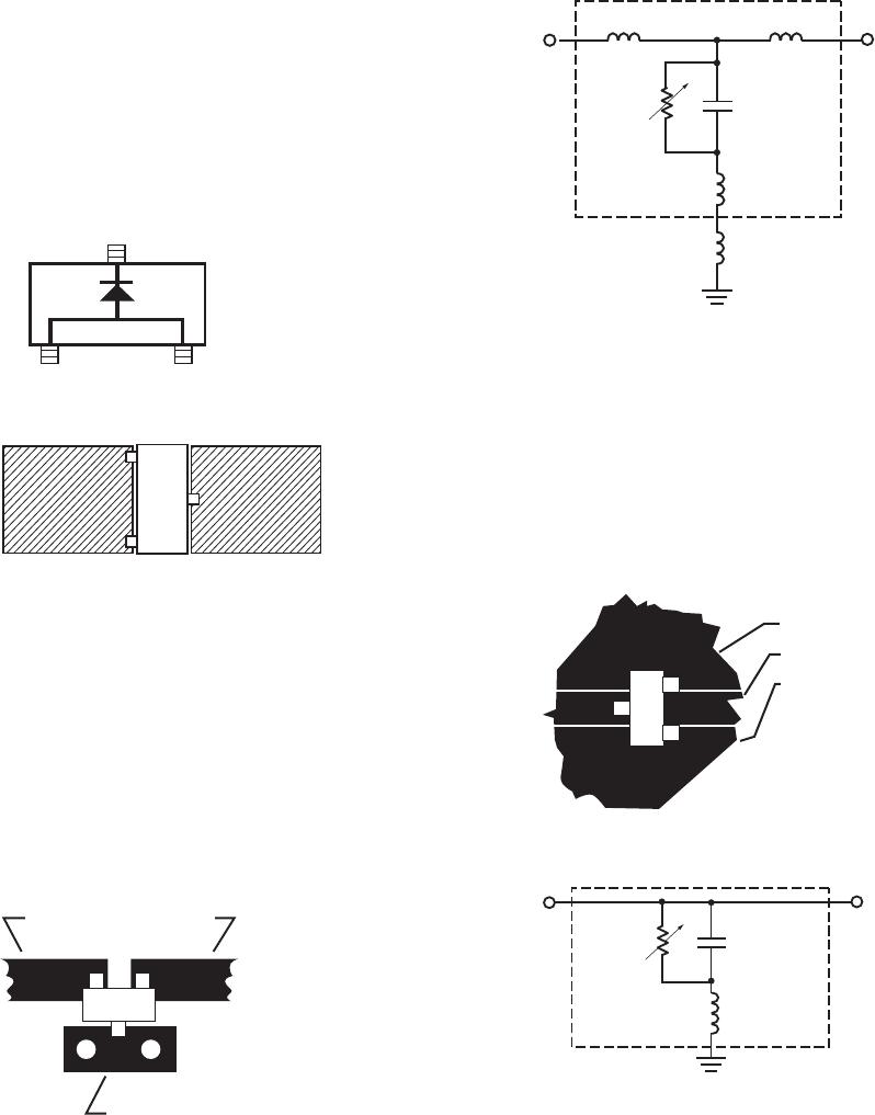
Figure 16. Equivalent Circuit.
Co-Planar Waveguide Shunt Connection for HSMP-482x Series
Co-Planar waveguide, with ground on the top side of
the printed circuit board, is shown in Figure 17. Since
it eliminates the need for via holes to ground, it o ers
lower shunt parasitic inductance and higher maximum
attenuation when compared to a microstrip circuit. See
AN1050 for details.
50 OHM MICROSTRIP LINES
PAD CONNECTED TO
GROUND BY TWO
VIA HOLES
0.3 nH
0.3 nH
0.8 pF
1.5 nH 1.5 nH
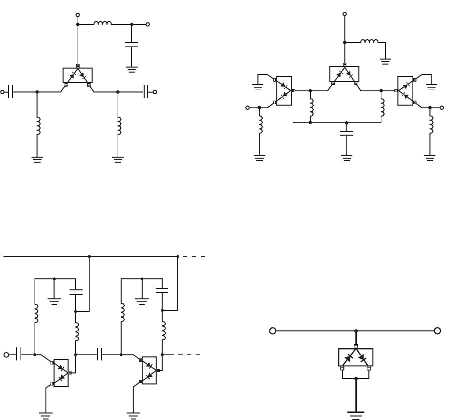
Figure 13. Internal Connections.
Figure 14. Circuit Layout.
Microstrip Shunt Connections for HSMP-482x Series
In Figure 15, the center conductor of the microstrip line
is interrupted and leads 1 and 2 of the HSMP-482x diode
are placed across the resulting gap. This forces the 0.5
nH lead inductance of leads 1 and 2 to appear as part of
a low pass lter, reducing the shunt parasitic inductance
and increasing the maximum available attenuation.
The 0.3 nH of shunt inductance external to the diode
is created by the via holes, and is a good estimate for
0.032" thick material.
Figure 15. Circuit Layout, HSMP-482x Limiter.
Figure 17. Circuit Layout.
Figure 18. Equivalent Circuit.
Co-Planar Waveguide
Groundplane
Groundplane
Center Conductor