LTC2954
13
2954fb
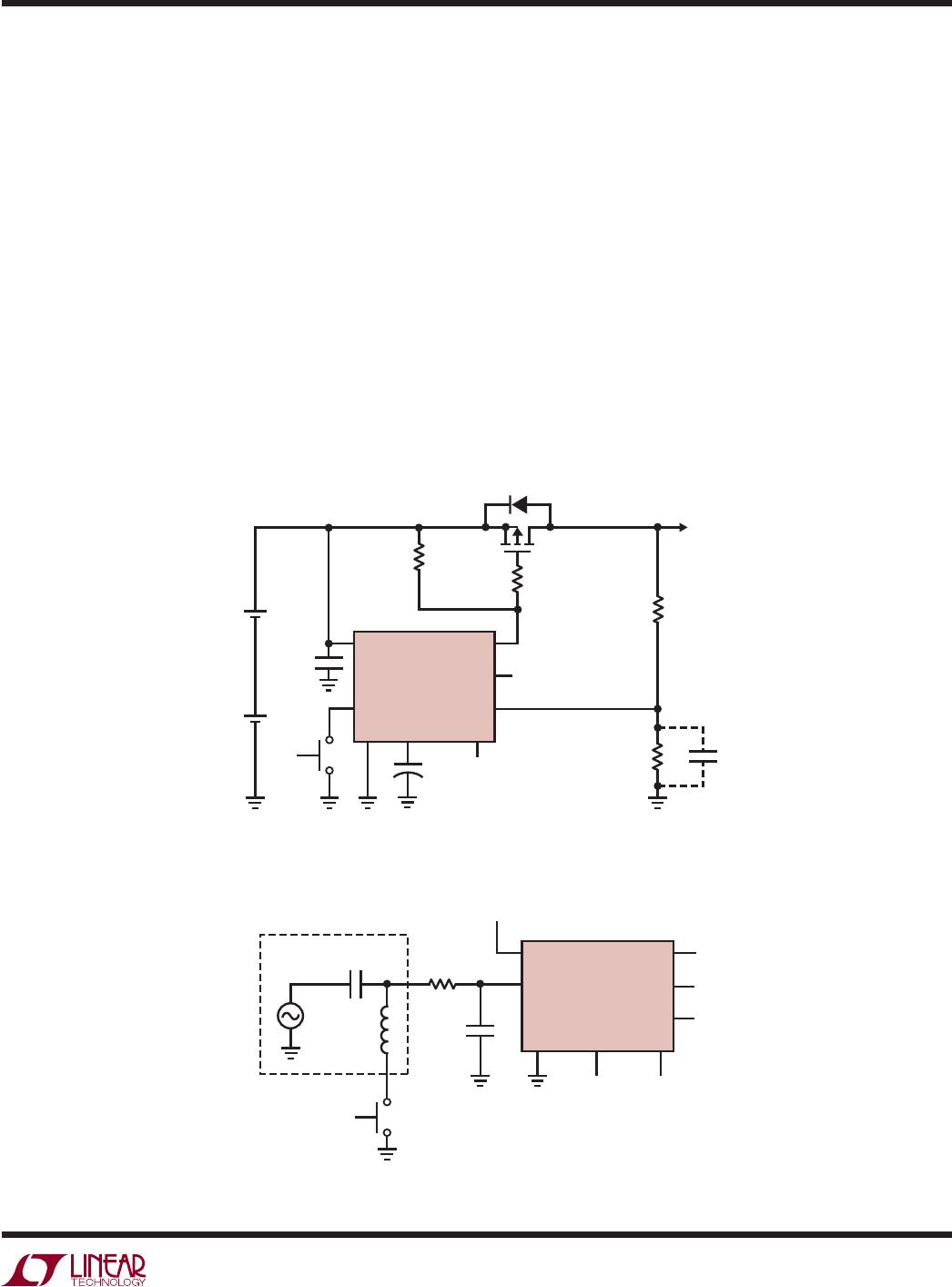
Figure 7. PowerPath Control with 6V Undervoltage Detect
width detected is 30μs. If there are glitches on the resis-
tor pull-up voltage that are wider than 30μs and transition
below 0.6V, then an appropriate bypass capacitor should
be connected to the KILL pin. The optional C
PDT
external
capacitor extends the length of time (beyond 64ms) that
the PB input must be held low before releasing the enable
output.
High Voltage PowerPath Switching
The high voltage EN open drain output of the LTC2954-2
is designed to switch on/off an external power PFET. This
allows a user to connect/disconnect a power supply (or
battery) to its load by toggling the PB pin. Figure 7 shows
the LTC2954-2 controlling a two cell Li-Ion battery ap-
plication. The KILL pin is connected to the output of the
TYPICAL APPLICATIONS
V
OUT
R1
909k
1%
R4
100k
1%
C3*
0.1μF
2954 F07
C4
0.1μF
CERAMIC
*OPTIONAL
V
TH
= 0.6V INPUT
R5
100k
R9
100k
M1
+
4.2V
SINGLE CELL
Li-Ion BATTERY
+
4.2V
SINGLE CELL
Li-Ion BATTERY
OPTIONAL GLITCH
FILTER CAPACITOR
V
OUT
,TRIP POINT = 6V
PB
EN
INT
KILL
LTC2954-2
GND ONT PDT
V
IN
C
ONT
*
0.033μF
PFET through a resistive divider. The KILL pin serves as
a voltage monitor. When V
OUT
drops below 6V, causing a
KILL voltage below V
KILL(TH)
, the EN pin becomes an open
circuit 30μs later. Since the PDT pin is open-circuited, the
power-down debounce time defaults to 64ms.
PB Pin in a Noisy Environment
The rugged PB pin is designed to operate in noisy environ-
ments. Transients below ground (>–6V) and above V
IN
(<33V) will not damage the rugged PB pin. Additionally,
the PB pin can withstand ESD HBM strikes up to ±10kV.
In order to keep external noise from coupling inside the
LTC2954, place an R-C network close to the PB pin. A 5.1k
resistor and a 0.1μF capacitor should suffice for most noisy
applications (see Figure 8).
Figure 8. Noisy PB Trace
PB
V
IN
LTC2954-1
GND ONT
R6
5.1k
2954 F08
TRACE
CAPACITANCE
PARASITICS
C5
0.1μF
DETAILS OMITTED
FOR CLARITY
TRACE
INDUCTANCE
NOISE
EN
INT
KILL
PDT
V
IN