LTC2954
9
2954fb
Description
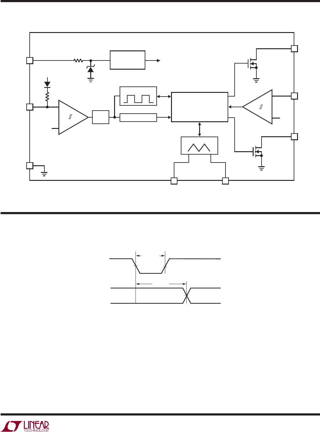
The LTC2954 is a pushbutton on/off controller that provides
control of system power via a pushbutton interface. An
enable output toggles system power while an interrupt
output provides debounced pushbutton status. The inter-
rupt output can be used in menu driven applications to
request a system power-down. A power kill input allows
a microprocessor or system to release the enable output,
effectively powering down the system. Independently ad-
justable on and off timers allow dependable pushbutton
control of the enable output and resistance to accidental
toggling of system power.
The length of time the pushbutton input (PB) must be held
low in order to toggle the enable (EN/EN) output on and
off is independently adjustable with external capacitors
at the ONT/PDT pins, respectively. During normal opera-
tion, the interrupt output (INT) is asserted 32ms after PB
goes low. INT then tracks PB until either PB or EN/EN is
released. See Timing Diagrams on page 8.
The KILL input is used to immediately release the enable
output. During a normal power-down sequence, INT re-
quests a system power-down. The μP then performs its
housekeeping tasks and then sets KILL low. If the μP fails
to set KILL low, the user can force a system shutdown by
pressing and holding the pushbutton until the PDT timer
expires.
Turn On
When power is first applied to the LTC2954, the part ini-
tializes the output pins. Any DC/DC converters connected
to the EN/EN pin will therefore be held off. To assert the
enable output, PB must be held low for a minimum of
32ms (t
DB
,
ON
). The LTC2954 provides additional turn-on
debounce time (t
ONT
) via an optional capacitor connected
to the ONT pin. The following equation describes the ad-
ditional time that PB must be held low before asserting the
enable output. C
ONT
is the ONT external capacitor (μF):
C
ONT
= 1.56 × 10
–4
[μF/ms] • (t
ONT
– 1ms)
Once the enable output is asserted, any DC/DC converters
connected to this pin are turned on. The KILL input from
the μP is ignored during a succeeding 512ms blanking
time (t
KILL,ON BLANK
). This blanking time represents the
maximum time required to power up the DC/DC converter
and the μP. If KILL is not brought high during this 512ms
time window, the enable output is released. The assump-
tion is that 512ms is sufficient time for the system to
power up.
Turn Off
To initiate a power-down sequence, assert the INT output
low by pressing the pushbutton for a minimum of 32ms
(t
DB,OFF
). The interrupt signal serves as a power-down
request to the μP. The μP would then perform power-down
and housekeeping tasks and assert KILL low when done.
This in turn releases the enable output, thus shutting off
system power.
Adjustable Power-Down Timer
The LTC2954 provides a failsafe feature that allows the
user to turn off system power (via PB) under system fault
conditions. For cases when the μP fails to respond to the
interrupt signal, the user can force an immediate power-
down by pressing and holding down the pushbutton. The
length of time that PB must be held low is given by a fixed
internal 64ms delay (t
PD,MIN
) plus an adjustable power-
down timer delay (t
PDT
, see Timing Diagrams on page 8).
The adjustable delay is set by placing an optional external
capacitor on the PDT pin. Use the following equation to
calculate the capacitance for the desired delay. C
PDT
is the
PDT external capacitor (μF):
C
PDT
= 1.56 × 10
-4
[μF/ms] • (t
PDT
– 1ms)
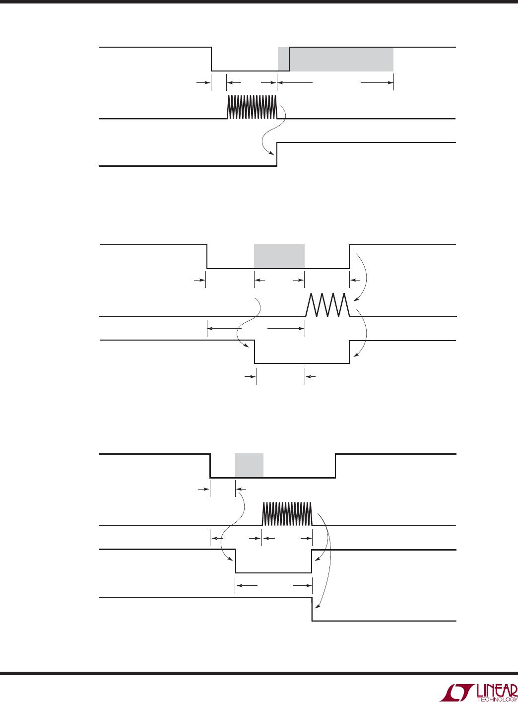
Simplified Power On/Off Sequence
Figure 1 shows a simplified LTC2954-1 power-on and
power-off sequence. A high to low transition on PB (t
1
)
initiates the power on sequence. In order to assert the
enable output, the PB pin must stay low continuously (PB
high resets timers) for a time controlled by the default
32ms and the external ONT capacitor (t
2
–t
1
). Once EN
goes high (t
2
), an internal 512ms blanking timer is started.
This blanking timer is designed to give sufficient time for
the DC/DC converter to reach its final voltage, and to allow
the μP enough time to perform power-on tasks.
The KILL pin must be pulled high within 512ms of the EN
pin going high. Failure to do so results in the EN pin going
APPLICATIONS INFORMATION