1
®
FN8184.1
CAUTION: These devices are sensitive to electrostatic discharge; follow proper IC Handling Procedures.
1-888-INTERSIL or 1-888-468-3774
| Intersil (and design) is a registered trademark of Intersil Americas Inc.
XDCP is a trademark of Intersil Americas Inc. Copyright Intersil Americas Inc. 2005. All Rights Reserved
All other trademarks mentioned are the property of their respective owners.
X9318
Digitally Controlled Potentiometer
(XDCP™)
FEATURES
Solid-state potentiometer
3-wire serial interface
Terminal voltage, 0 to +8V
100 wiper tap points
Wiper position stored in nonvolatile memory
and recalled on power-up
99 resistive elements
Temperature compensated
End to end resistance range ± 20%
Low power CMOS
—V
CC
= 5V
Active current, 3mA max.
Standby current, 1mA max.
High reliability
Endurance, 100,000 data changes per bit
Register data retention, 100 years
•R
TOTAL
value = 10k
Packages
8 Ld SOIC and DIP
Pb-free plus anneal available (RoHS compliant)
APPLICATIONS
LCD bias control
DC bias adjustment
Gain and offset trim
Laser diode bias control
Voltage regulator output control
DESCRIPTION
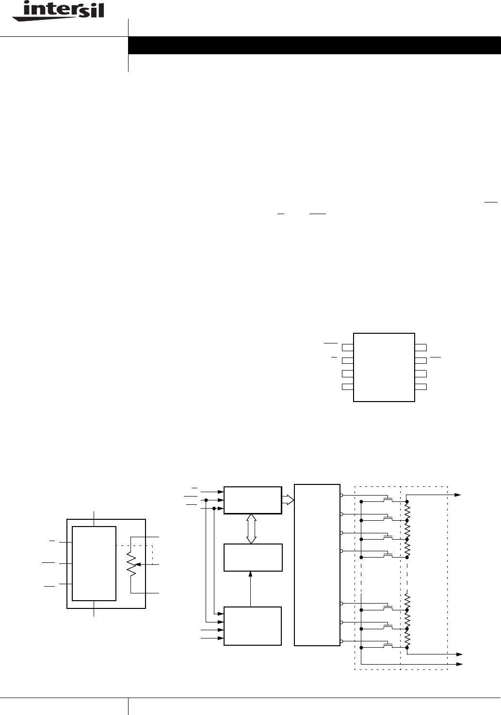
The Intersil X9318 is a digitally controlled potentiometer
(XDCP). The device consists of a resistor array, wiper
switches, a control section, and nonvolatile memory.
The wiper position is controlled by a 3-wire interface.
The potentiometer is implemented by a resistor array
composed of 99 resistive elements and a wiper switch-
ing network. Between each element and at either end
are tap points accessible to the wiper terminal. The
position of the wiper element is controlled by the CS
,
U/D
, and INC inputs. The position of the wiper can be
stored in nonvolatile memory and then be recalled
upon a subsequent power-up operation.
The device can be used as a three-terminal potentiome-
ter for voltage control or as a two-terminal variable resis-
tor for current control in a wide variety of applications.
PIN CONFIGURATION
BLOCK DIAGRAM
R
H
V
CC
INC
U/D
1
2
3
4
8
7
6
5
X9318
DIP/SOIC
V
SS
CS
R
L
R
W
Up/Down
Counter
7-Bit
Nonvolatile
Memory
Store and
Recall
Control
Circuitry
One
of
One
Decoder
Resistor
Array
R
H
U/D
INC
CS
Wiper
Switches
Hundred
V
CC
V
SS
R
L
R
W
Control
and
Memory
Up/Down
(U/D
)
Increment
(INC
)
Device Select
(CS
)
V
CC
(Supply Voltage)
V
SS
(Ground)
R
H
R
W
R
L
General
Detailed
0
1
2
96
97
98
99
Data Sheet September 14, 2005
2
FN8184.1
September 14, 2005
PIN DESCRIPTIONS
Ordering Information
PART NUMBER PART MARKING R
TOTAL
(k) TEMP RANGE (°C) PACKAGE
X9318WP8 X9318WP 10 0 to 70 8 Ld PDIP
X9318WP8I X9318WP I -40 to 85 8 Ld PDIP
X9318WS8* X9318W 0 to 70 8 Ld SOIC (150 mil)
X9318WS8Z* (Note) X9318W Z 0 to 70 8 Ld SOIC (150 mil) (Pb-free)
X9318WS8I* X9318W I -40 to 85 8 Ld SOIC (150 mil)
X9318WS8IZ* (Note) X9318W Z I -40 to 85 8 Ld SOIC (150 mil) (Pb-free)
*Add "T1" suffix for tape and reel.
NOTE: Intersil Pb-free plus anneal products employ special Pb-free material sets; molding compounds/die attach materials and 100% matte tin plate
termination finish, which are RoHS compliant and compatible with both SnPb and Pb-free soldering operations. Intersil Pb-free products are MSL
classified at Pb-free peak reflow temperatures that meet or exceed the Pb-free requirements of IPC/JEDEC J STD-020.
DIP/SOIC Symbol Brief Description
1INCIncrement. Toggling INC while CS is low moves the wiper either up or down.
2U/D
Up/Down. The U/D input controls the direction of the wiper movement.
3R
H
The high terminal is equivalent to one of the fixed terminals of a mechanical potentiometer.
4V
SS
Ground.
5R
W
The wiper terminal is equivalent to the movable terminal of a mechanical potentiometer.
6
R
L
The low terminal is equivalent to one of the fixed terminals of a mechanical potentiometer.
7CS
Chip Select. The device is selected when the CS input is LOW, and de-selected when CS is high.
8V
CC
Supply Voltage.
X9318
3
FN8184.1
September 14, 2005
ABSOLUTE MAXIMUM RATINGS
Junction Temperature under bias...... -65°C to +135°C
Storage temperature ......................... -65°C to +150°C
Voltage on CS
, INC, U/D and V
CC
with respect to V
SS
................................. -1V to +7V
R
H
, R
W
, R
L
to ground..........................................+10V
Lead temperature (soldering 10s) ..................... 300°C
I
W
(10s)..............................................................±6mA
COMMENT
Stresses above those listed under “Absolute Maximum
Ratings” may cause permanent damage to the device.
This is a stress rating only; functional operation of the
device (at these or any other conditions above those
listed in the operational sections of this specification) is
not implied. Exposure to absolute maximum rating con-
ditions for extended periods may affect device reliability.
POTENTIOMETER CHARACTERISTICS
(V
CC
= 5V ± 10%, T
A
= Full Operating Temperature Range unless otherwise stated)
Symbol Parameter
Limits
Test Conditions/NotesMin. Typ.
(4)
Max. Unit
End to end resistance tolerance -20 +20 % See ordering information
for values
V
RH
/
RL
R
H
/R
L
terminal voltage V
SS
8VV
SS
= 0V
Power rating 25 mW
R
W
Wiper resistance 40 200 I
W
= 1mA
I
W
Wiper current
(5)
-3.0 +3.0 mA See test circuit
Noise
(7)
-120 dBV Ref: 1kHz
Resolution 1 %
Absolute linearity
(1)
-1 +1 MI
(3)
V(RH) = 8V,
V(RL) = 0V
Relative linearity
(2)
-0.2 +0.2 MI
(3)
R
TOTAL
temperature coefficient
(5)
±300 ppm/°C
Ratiometric temperature coeffi-
cient
(5),(6)
-20 +20 ppm/°C
C
H
/C
L
/C
W
(5
)
Potentiometer capacitances 10/10/25 pF See equivalent circuit
V
CC
Supply Voltage 4.5 5.5 V
X9318

X9318WS8IZ

Mfr. #:
Manufacturer:
Renesas / Intersil
Description:
Digital Potentiometer ICs 100-TAP 10KOHMUP/DWN INTERFA NON-VOLATILE
Lifecycle:
New from this manufacturer.
Delivery:
DHL FedEx Ups TNT EMS
Payment:
T/T Paypal Visa MoneyGram Western Union