6
FN8184.1
September 14, 2005
PIN DESCRIPTIONS
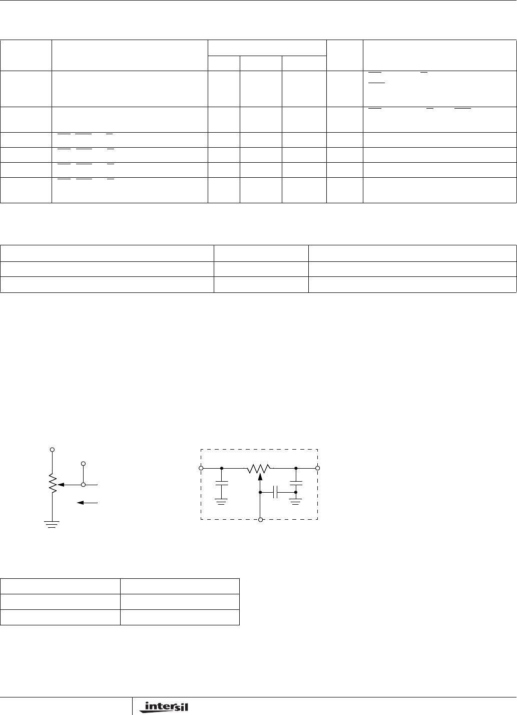
R
H
and R
L
The high (R
H
) and low (R
L
) terminals of the X9318 are
equivalent to the fixed terminals of a mechanical
potentiometer. The terminology of R
L
and R
H
refer-
ences the relative position of the terminal in relation to
wiper movement direction selected by the U/D
input
and not the voltage potential on the terminal.
R
W
R
w
is the wiper terminal and is equivalent to the mov-
able terminal of a mechanical potentiometer. The posi-
tion of the wiper within the array is determined by the
control inputs. The wiper terminal series resistance is
typically 40Ω.
Up/Down (U/D
)
The U/D
input controls the direction of the wiper move-
ment and whether the counter is incremented or dec-
remented.
Increment (INC
)
The INC
input is negative-edge triggered. Toggling
INC
will move the wiper and either increment or decre-
ment the counter in the direction indicated by the logic
level on the U/D
input.
Chip Select (CS
)
The device is selected when the CS
input is LOW. The
current counter value is stored in nonvolatile memory
when CS
is returned HIGH while the INC input is also
HIGH. After the store operation is complete the X9318
will be placed in the low power standby mode until the
device is selected once again.
PIN CONFIGURATION
PIN NAMES
PRINCIPLES OF OPERATION
There are three sections of the X9318: the control
section, the nonvolatile memory, and the resistor
array. The control section operates just like an
up/down counter. The output of this counter is
decoded to turn on a single electronic switch
connecting a point on the resistor array to the wiper
output. The contents of the counter can be stored in
nonvolatile memory and retained for future use. The
resistor array is comprised of 99 individual resistors
connected in series. Electronic switches at either end
of the array and between each resistor provide an
electrical connection to the wiper pin, R
W
.
The wiper acts like its mechanical equivalent and does
not move beyond the first or last position. That is, the
counter does not wrap around when clocked to either
extreme.
The electronic switches on the device operate in a
“make before break” mode when the wiper changes
tap positions. If the wiper is moved several positions,
multiple taps are connected to the wiper for t
IW
(INC to
V
W
change). The R
TOTAL
value for the device can
temporarily be reduced by a significant amount if the
wiper is moved several positions.
When the device is powered-down, the last wiper posi-
tion stored will be maintained in the nonvolatile mem-
ory. When power is restored, the contents of the
memory are recalled and the wiper is set to the value
last stored.
R
H
V
CC
INC
U/D
1
2
3
4
8
7
6
5
X9318
DIP/SOIC
V
SS
CS
R
L
R
W
Symbol Description
R
H
High terminal
R
W
Wiper terminal
R
L
Low terminal
V
SS
Ground
V
CC
Supply voltage
U/D Up/Down control input
INC
Increment control input
CS
Chip select control input
X9318