www.irf.com © 2014 International Rectifier Submit Datasheet Feedback March 27, 2014
2
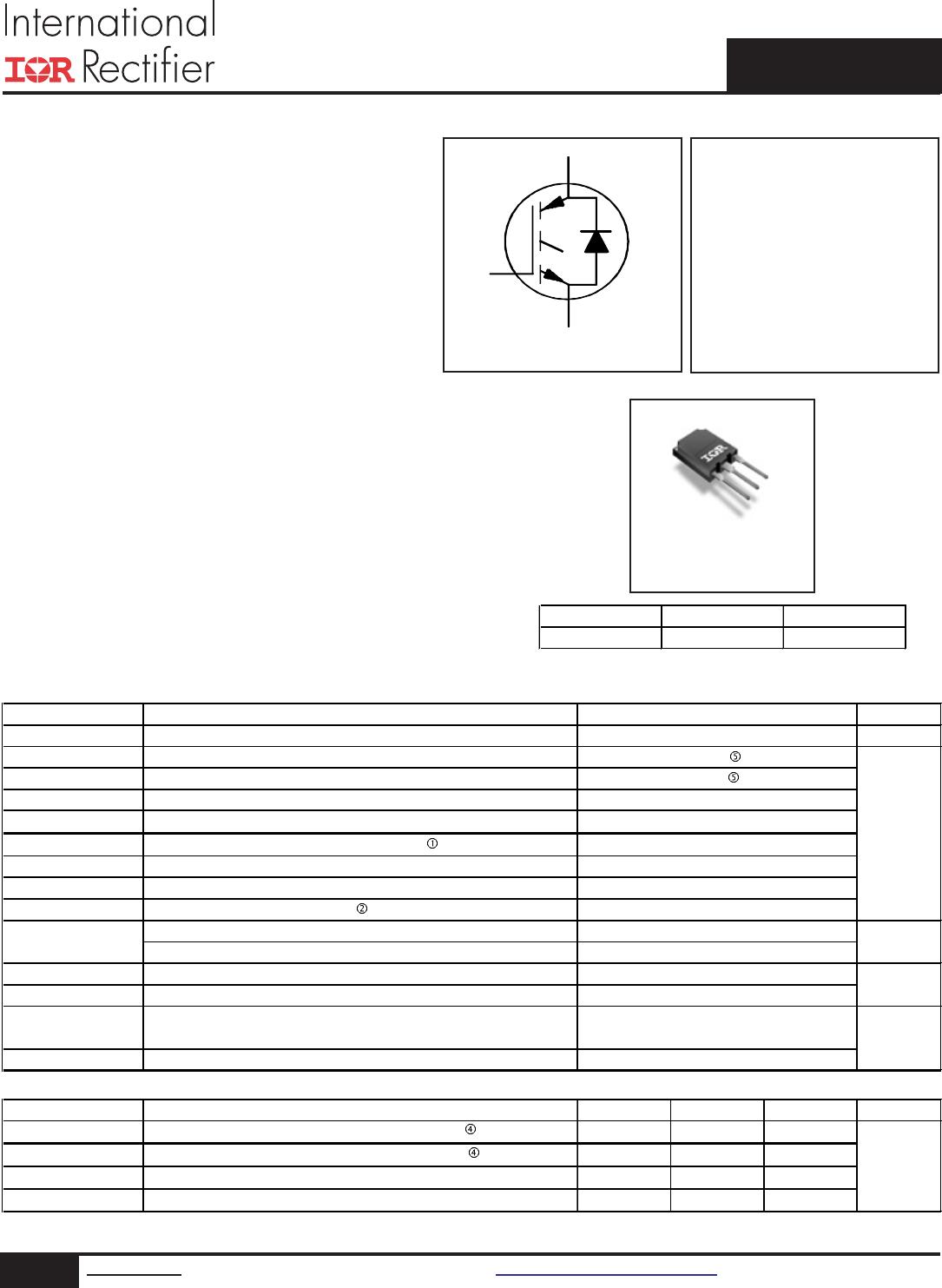
IRGPS4067DPbF
Notes:
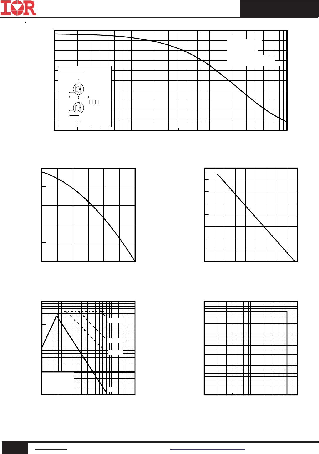
V
CC
= 80% (V
CES
), V
GE
= 20V, L = 66µH, R
G
= 4.7Ω, tested in production I
LM
≤ 400A.
Pulse width limited by max. junction temperature.
Refer to AN-1086 for guidelines for measuring V
(BR)CES
safely.
R
θ
is measured at T
J
of approximately 90°C.
Calculated continuous current based on maximum allowable junction temperature. Package IGBT current limit is 195A. Package diode current
limit is 120A. Note that current limitations arising from heating of the device leads may occur.
Maximum limits are based on statistical sample size characterization.
Electrical Characteristics @ T
J
= 25°C (unless otherwise specified)
Parameter Min. Typ. Max. Units Conditions
V
(BR)CES
Collector-to-Emitter Breakdown Vol tage
600 — — V V
GE
= 0V, I
C
= 100µA
∆
V
(B R)CE S
/
∆
T
J
T emper atur e Coef f. of B r eakdown Vo l tage
—0.27—V/°CV
GE
= 0V, I
C
= 4.0mA (25°C-175°C)
— 1.70 2.05 I
C
= 120A, V
GE
= 15V, T
J
= 25°C
V
CE(on)
Collector-to-Emitter Saturation Voltage — 2.15 — V I
C
= 120A, V
GE
= 15V, T
J
= 150°C
—2.20— I
C
= 120A, V
GE
= 15V, T
J
= 175°C
V
GE (t h)
Gate Threshold Voltage 4.0 — 6.5 V V
CE
= V
GE
, I
C
= 5.6mA
∆
V
GE ( t h )
/
∆
TJ
Threshold Voltage temp. coefficient — -17 — mV/°C V
CE
= V
GE
, I
C
= 5.6mA (25°C - 175°C)
gfe Forward Transconductance — 77 — S V
CE
= 50V, I
C
= 120A
I
CES
Collector-to-Emitter Leakage Current — 1.0 150 µA V
GE
= 0V, V
CE
= 600V
—2.3—mAV
GE
= 0V, V
CE
= 600V, T
J
= 175°C
V
FM
Diode Forward Voltage Drop — 2.4 3.0 V I
F
= 120A
—1.9— I
F
= 120A, T
J
= 175°C
I
GE S
Gate-to-Emitter Leakage Current — — ±400 nA V
GE
= ±20V
Switching Characteristics @ T
J
= 25°C (unless otherwise specified)
Parameter Min. Typ. Max. Units
Q
g
Total Gate Charge (turn-on) — 240 360 I
C
= 120A
Q
ge
Gate-to-Emitter Charge (turn-on) — 70 105 nC V
GE
= 15V
Q
gc
Gate-to-Collector Charge (turn-on) — 90 135 V
CC
= 400V
E
on
Turn-On Switching Loss — 5750 7990 I
C
= 120A, V
CC
= 400V, V
GE
= 15V
E
off
Turn-Off Switching Loss — 3430 4360 µJ R
G
= 4.7
Ω
, L = 66µH, T
J
= 25°C
E
total
Total Switching Loss — 9180 12350
Energy los s es include tail & diode reverse recovery
t
d(on)
Turn-On delay time — 80 100 I
C
= 120A, V
CC
= 400V, V
GE
= 15V
t
r
Rise time — 70 125 ns R
G
= 4.7
Ω
, L = 66µH, TJ = 25°C
t
d(off)
Turn-Off delay time — 190 220
t
f
Fall time — 40 60
E
on
Turn-On Switching Loss — 7740 — I
C
= 120A, V
CC
= 400V, V
GE
=15V
E
off
Turn-Off Switching Loss — 4390 — µJ R
G
=4.7
Ω
, L=66µH, T
J
= 175°C
E
total
Total Switching Loss — 12130 —
Energy los s es include tail & diode reverse recovery
t
d(on)
Turn-On delay time — 80 — I
C
= 120A, V
CC
= 400V, V
GE
= 15V
t
r
Rise time — 75 — ns R
G
= 4.7
Ω
, L = 66µH
t
d(off)
Turn-Off delay time — 230 — T
J
= 175°C
t
f
Fall time — 55 —
C
ies
Input Capacitance — 7750 — pF V
GE
= 0V
C
oes
Output Capacitance — 550 — V
CC
= 30V
C
res
Reverse Transfer Capacitance — 225 — f = 1.0Mhz
T
J
= 175°C, I
C
= 480A
RBSOA Reverse Bias Safe Operating Area FULL SQUARE V
CC
= 480V, Vp =600V
Rg = 4.7
Ω
, V
GE
= +20V to 0V
SCSOA Short Circuit Safe Operating Area 5 — — µs V
CC
= 400V, Vp =600V
Rg = 4.7
Ω
, V
GE
= +15V to 0V
Erec Reverse Recovery Energy of the Diode — 500 — µJ T
J
= 175°C
t
rr
Diode Reverse Recovery Time — 130 — ns V
CC
= 400V, I
F
= 120A
I
rr
Peak Reverse Recovery Current — 36 — A V
GE
= 15V, Rg = 4.7
Ω
, L =100µH
Conditions