ADRF5040 Data Sheet
Rev. A | Page 12 of 14
THEORY OF OPERATION
The ADRF5040 requires a positive supply voltage applied to the
V
DD
pin and a negative voltage supply applied to the V
SS
pin.
Bypassing capacitors are recommended on the supply lines to
minimize RF coupling.
The ADRF5040 is controlled via two digital control voltages
applied to the V
1
pin and the V
2
pin. A small value bypassing
capacitor is recommended on these digital signal lines to
improve the RF signal isolation.
The ADRF5040 is internally matched to 50 Ω at the RF input
port (RFC) and the RF output ports (RF1, RF2, RF3, and RF4);
therefore, no external matching components are required. The
RF1 through RF4 pins are dc-coupled, and dc blocking capacitors
are required on the RF paths. The design is bidirectional; the
input and outputs are interchangeable.
The ADRF5040 does not need any special power-up sequencing,
and the relative order to power up the V
DD
and V
SS
supplies is not
important. The V
1
and V
2
control signals can be applied only
after V
DD
is powered up; this sequence avoids forward biasing
and causing damage to the internal ESD protection circuits.
Turn on the RF signal after the device supply settles to a steady
state.
Data Sheet ADRF5040
Rev. A | Page 13 of 14
APPLICATIONS INFORMATION
EVALUATION BOARD
The ADRF5040-EVAL Z evaluation board shown in Figure 27 is
designed using proper RF circuit design techniques. Signal lines
at the RF port have 50 impedance, and the package ground
leads and backside ground slug must be connected directly to
the ground plane. The evaluation board is available from Analog
Devices, Inc. upon request.
RF1
RF2
VDD
V1
GND
THRU CAL
600-00598-00-3
V2
VSS
RF4
RFC
RF3
J4
J5
J2
J1
U1
J3
C1 C6
14290-027
Figure 27. Evaluation PCB
Table 7. Bill of Materials for the ADRF5040-EVALZ Evaluation Board
Item Description
J1 to J5 PC mount SMA RF connectors
TP1 to TP5 Through hole mount test points
C1, C6 100 pF capacitors, 0402 package
U1 ADRF5040 SP4T switch
PCB 600-00598-00-3 evaluation PCB, Rogers 4350 circuit board material
ADRF5040 Data Sheet
Rev. A | Page 14 of 14
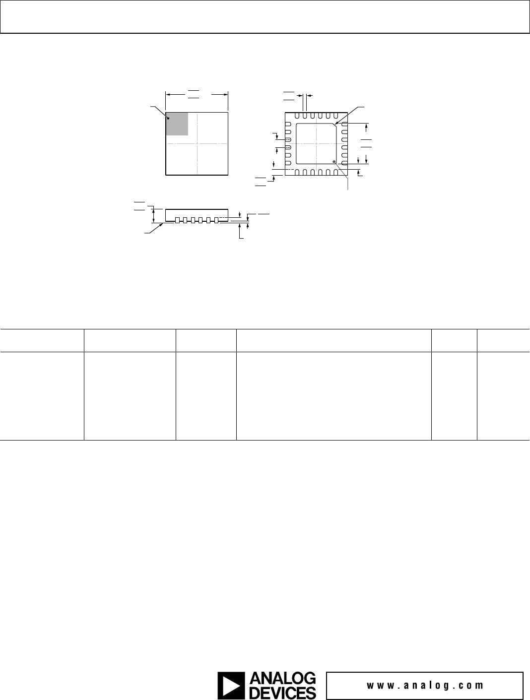
OUTLINE DIMENSIONS
0.50
BSC
0.50
0.40
0.30
COMPLIANT
TO
JEDEC STANDARDS MO-220-VGGD-8.
BOTTOM VIEW
TOP VIEW
4.10
4.00 SQ
3.90
SEATING
PLANE
0.90
0.85
0.80
0.05 MAX
0.02 NOM
0.20 REF
COPLANARITY
0.08
PIN 1
INDICATOR
1
24
7
12
13
18
19
6
FOR PROPER CONNECTION OF
THE EXPOSED PAD, REFER TO
THE PIN CONFIGURATION AND
FUNCTION DESCRIPTIONS
SECTION OF THIS DATA SHEET.
05-25-2016-B
0.30
0.25
0.18
PIN 1
INDICATOR
0.20 MIN
2.85
2.70 SQ
2.55
EXPOSED
PAD
PKG-004926/PKG-004866
Figure 28. 24-Lead Lead Frame Chip Scale Package [LFCSP]
4 mm × 4 mm Body and 0.85 mm Package Height
(CP-24-16)
Dimensions shown in millimeters
ORDERING GUIDE
Model
1
Temperature Range MSL Rating
2
Package Description
Package
Option Branding
3
ADRF5040BCPZ 40°C to +85°C MSL3 24-Lead Lead Frame Chip Scale Package [LFCSP] CP-24-16
XXXXX#
5040
ADRF
ADRF5040BCPZ-R7 −40°C to +85°C MSL3 24-Lead Lead Frame Chip Scale Package [LFCSP] CP-24-16
XXXXX#
5040
ADRF
ADRF5040-EVALZ Evaluation Board
1
These models are RoHS Compliant Parts.
2
See the Absolute Maximum Ratings section.
3
XXXXX is the 5-digit lot number.
©2016–2017 Analog Devices, Inc. All rights reserved. Trademarks and
registered trademarks are the property of their respective owners.
D14290-0-2/17(A)

ADRF5040BCPZ

Mfr. #:
Manufacturer:
Analog Devices Inc.
Description:
RF Switch ICs High isolation, SP4T, 9kHz - 12GHz
Lifecycle:
New from this manufacturer.
Delivery:
DHL FedEx Ups TNT EMS
Payment:
T/T Paypal Visa MoneyGram Western Union

Products related to this Datasheet