ADRF5040 Data Sheet
Rev. A | Page 6 of 14
PIN CONFIGURATION AND FUNCTION DESCRIPTIONS
PACKAGE
BASE
GND
2
1
3
4
5
6
18
17
16
15
14
13
GND
GND
GND
RFC
GND
GND
GND
V
SS
V
2
V
1
V
DD
GND
8
9
10
11
7
RF4
GND
GND
RF3
12
GND
GND
20
19
21
RF2
GND
GND
22
GND
23
RF1
24
GND
ADRF5040
TOP VIEW
(Not to Scale)
NOTES
1. EXPOSED PAD. THE EXPOSED PAD MUST BE
CONNECTED TO THE RF/DC GROUND OF THE
PRINTED CIRCUIT BOARD (PCB).
14290-005
Figure 5. Pin Configuration
Table 5. Pin Function Descriptions
Pin No. Mnemonic Description
1, 2, 4 to 7, 9, 10, 12, 13,
18, 19, 21, 22, 24
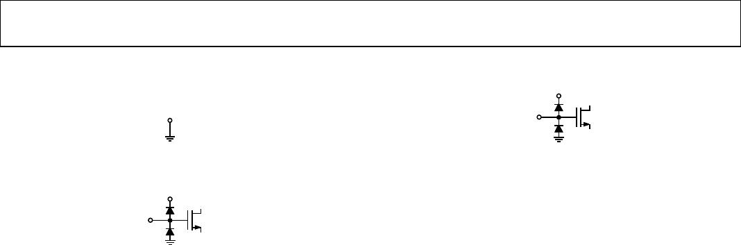
GND Ground. The package bottom has an exposed metal pad that must connect to the printed circuit
board (PCB) RF/dc ground. See Figure 6 for the GND interface schematic.
3 RFC RF Common Port. This pin is dc-coupled and matched to 50 Ω. A dc blocking capacitor is required
if the RF line potential is not equal to 0 V dc.
8 RF4 RF4 Port. This pin is dc-coupled and matched to 50 Ω. A dc blocking capacitor is required if the RF
line potential is not equal to 0 V dc.
11 RF3 RF3 Port. This pin is dc-coupled and matched to 50 Ω. A dc blocking capacitor is required if the RF
line potential is not equal to 0 V dc.
14 V
SS
Negative Supply Voltage Pin.
15 V
2
Control Input Pin 2. See Table 2 and Table 6.
16 V
1
Control Input Pin 1. See Table 2 and Table 6.
17 V
DD
Positive Supply Voltage.
20 RF2 RF2 Port. This pin is dc-coupled and matched to 50 Ω. A dc blocking capacitor is required if the RF
line potential is not equal to 0 V dc.
23 RF1 RF1 Port. This pin is dc-coupled and matched to 50 Ω. A dc blocking capacitor is required if the RF
line potential is not equal to 0 V dc.
EPAD Exposed Pad. The exposed pad must be connected to the RF/dc ground of the PCB.
Table 6. Truth Table
Digital Control Inputs
Signal Path State
V
1
V
2
Low Low RFC to RF1
High Low RFC to RF2
Low High RFC to RF3
High High RFC to RF4