MAX9597
Low-Power Audio/Video Interface
for Single SCART Connectors
______________________________________________________________________________________ 19
when the MAX9597 is operating without loads and with-
out any audio or video signals. Table 4 shows the qui-
escent power consumption in both operating modes.
Average power consumption is defined when the
MAX9597 drives typical signals into typical loads. Table 5
shows the average power consumption in full-power
mode, and Table 6 shows the input and output conditions.
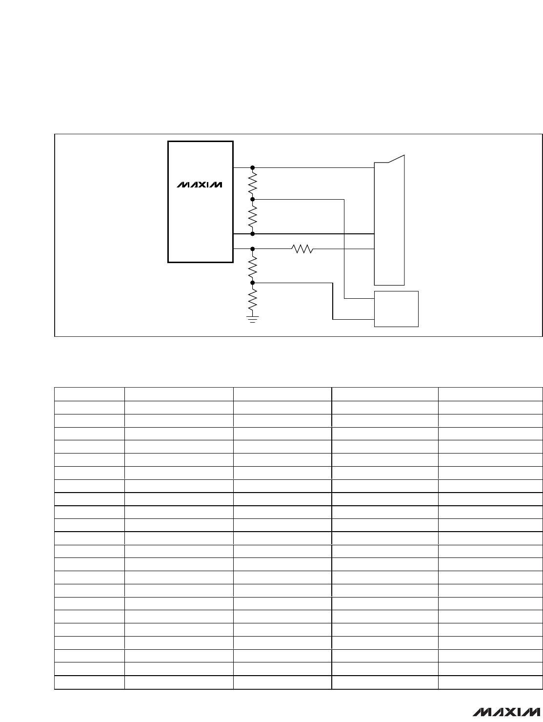
Interfacing to an RF Modulator
If the set-top box modulates CVBS and mono audio
onto an RF carrier (for example, channel 3), a simple
application circuit can provide the needed signals (see
Figure 11). A 10k resistor summer circuit between
TV_OUTR and TV_OUTL creates the mono audio sig-
nal. The resistor-divider to ground on TV_CVBS_OUT
creates a video signal with normal amplitude. The
unique feature of the MAX9597 that facilitates this
application circuit is that the audio and video output
amplifiers of the MAX9597 can drive multiple loads if
V
AUD
and V
VID
are both greater than 3.135V.
Floating-Chassis Discharge Protection
and ESD
Some set-top boxes have a floating chassis problem in
which the chassis is not connected to earth ground. As
a result, the chassis can charge up to 500V. When a
SCART cable is connected to the SCART connector,
the charged chassis can discharge through a signal
pin. The equivalent circuit is a 2200pF capacitor
charged to 311V connected through less than 0.1 to a
signal pin. The MAX9597 is soldered on the PCB when
it experiences such a discharge. Therefore, the current
spike flows through both external and internal ESD pro-
tection devices and is absorbed by the supply bypass
capacitors, which have high capacitance and low ESR.
ACKNOWLEDGE FROM MAX9597
1 BYTE
AUTOINCREMENT INTERNAL
REGISTER ADDRESS POINTER
ACKNOWLEDGE FROM MAX9597
NOT ACKNOWLEDGE FROM MASTER
AA
P
A
0
ACKNOWLEDGE FROM MAX9597
R/W
SA
R/WREPEATED START
Sr 1SLAVE ADDRESS REGISTER ADDRESS SLAVE ADDRESS DATA BYTE
Figure 9. Reading One Indexed Byte of Data from the MAX9597
ACKNOWLEDGE FROM MAX9597
1 BYTE
AUTOINCREMENT INTERNAL
REGISTER ADDRESS POINTER
ACKNOWLEDGE FROM MAX9597
AA
AP
0
ACKNOWLEDGE FROM MAX9597
R/W
SA
R/W
REPEATED START
Sr 1SLAVE ADDRESS REGISTER ADDRESS SLAVE ADDRESS DATA BYTE
Figure 10. Reading n-Bytes of Indexed Data from the MAX9597
OPERATING MODE POWER CONSUMPTION (mW)
Shutdown 0.005
Full power 53
Table 4. Quiescent Power Consumption
OPERATING MODE POWER CONSUMPTION (mW)
Full power 254
Table 5. Average Power Consumption
MAX9597
Low-Power Audio/Video Interface
for Single SCART Connectors
20 ______________________________________________________________________________________
TV
SCART
MAX9597
TV_OUTR
TV_OUTL
10k
10k
MONO AUDIO
TV_CVBS_OUT
75 OR GREATER
75 OR GREATER
75
RF
MODULATOR
Figure 11. Application Circuit to Connect CVBS and Mono Audio from TV SCART to RF Modulator
PIN NAME TYPE SIGNAL LOAD
1V
AUD
Supply 3.3V N/A
8 ENC_B_IN Input 50% flat field N/A
9 ENC_G_IN Input 50% flat field N/A
10 ENC_R/C_IN Input 50% flat field N/A
11 ENC_CVBS_IN Input 50% flat field N/A
12 TV_CVBS_OUT Output 50% flat field 150 to ground
13 V
VID
Supply 3.3V N/A
14 TV_FS_OUT Output 3.3V 150 to ground
15 GND Supply 0 N/A
16 TV_R/C_OUT Output 50% flat field 150 to ground
17 TV_G_OUT Output 50% flat field 150 to ground
18 TV_B_OUT Output 50% flat field 150 to ground
19 V
12
Supply 12V N/A
20 TV_SS_OUT Output 12V 10k to ground
21 TV_OUTL Output 1V
RMS
, 1kHz 10k to ground
22 ENC_INL+ Input 0.25V
RMS
, 1kHz N/A
23 ENC_INL- Input N/A N/A
24 ENC_INLOUT Output N/A 1k to ground
25 ENC_INROUT Output N/A 1k to ground
26 ENC_INR- Input N/A N/A
27 ENC_INR+ Input 0.25V
RMS
, 1kHz N/A
28 TV_OUTR Output 1V
RMS
, 1kHz 10k to ground
Table 6. Conditions for Average Power Consumption Measurement
Note: Input operational amplifiers set to unity-gain configuration.
MAX9597
Low-Power Audio/Video Interface
for Single SCART Connectors
______________________________________________________________________________________ 21
MAX9597
SDA
SCL
DEV_ADDR
TV
SCART
V
12
0.1µF
12V
V
VID
0.1µF
ENC_CVBS_IN
75
ENC_R/C_IN
75
ENC_G_IN
75
ENC_B_IN
75
3.3V
+3.3V
V
AUD
0.1µF
3.3V
ENC_INLOUT
ENC_INR+
ENC_INL+
ENC_INL-
ENC_INR-
ENC_INROUT
VIDEO
ENCODER
µC
STB CHIP
STEREO
AUDIO
DACS WITH
DIFFERENTIAL
OUTPUTS
TV_OUTR
300
V
AUD
CPV
SS
TV_OUTL
300
V
AUD
CPV
SS
TV_SS_OUT
100
V
12
EP
TV_B_OUT
75
V
VID
GND
TV_G_OUT
75
V
VID
GND
TV_R/C_OUT
75
V
VID
GND
TV_FS_OUT
75
V
VID
GND
TV_CVBS_OUT
C1P
C1N
CPVSS
GND
EP
75
V
VID
GND
124 15nF
124
15nF
124
15nF
124
15nF
NOTE: OPTIONAL RESISTOR CAN BE PLACED
FROM AUDIO DAC OUTPUTS TO GROUND TO
DECREASE SWING AT AUDIO DAC OUTPUTS.
:BAV99, SMALL-SIGNAL DIODE
Figure 12. Application Circuit to Connect Series Resistors and External ESD Protection Diodes at MAX9597 Outputs

MAX9597CTI+T

Mfr. #:
Manufacturer:
Maxim Integrated
Description:
Multimedia ICs Video ICs A/V Switch for Dual SCART Connecto
Lifecycle:
New from this manufacturer.
Delivery:
DHL FedEx Ups TNT EMS
Payment:
T/T Paypal Visa MoneyGram Western Union

Products related to this Datasheet