TFF11092HN All information provided in this document is subject to legal disclaimers. © NXP B.V. 2013. All rights reserved.
Product data sheet Rev. 1 — 28 March 2013 10 of 17
NXP Semiconductors
TFF11092HN
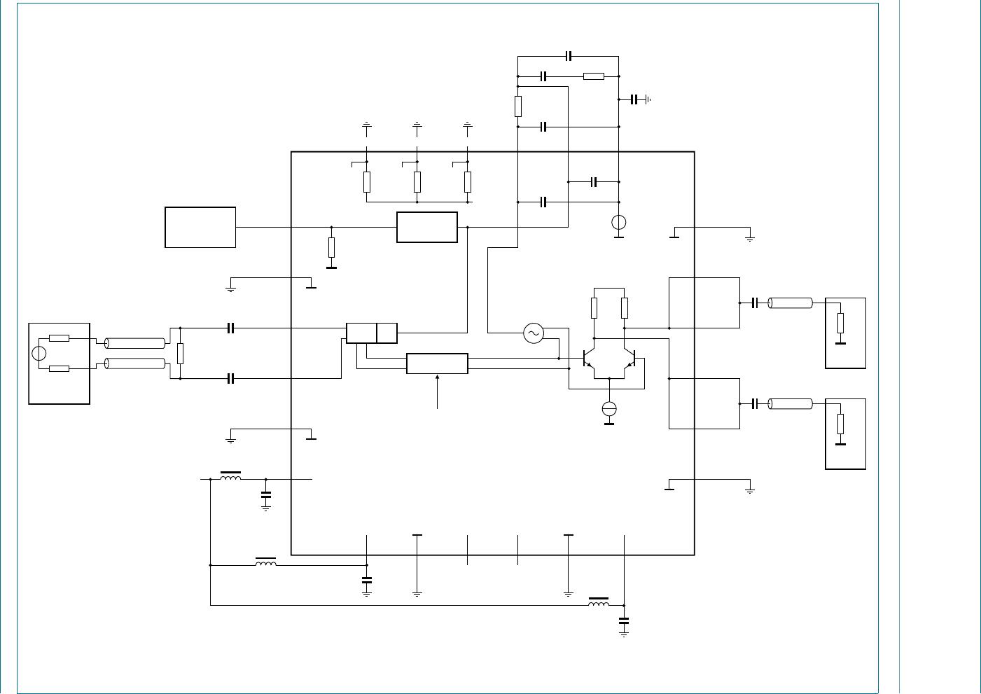
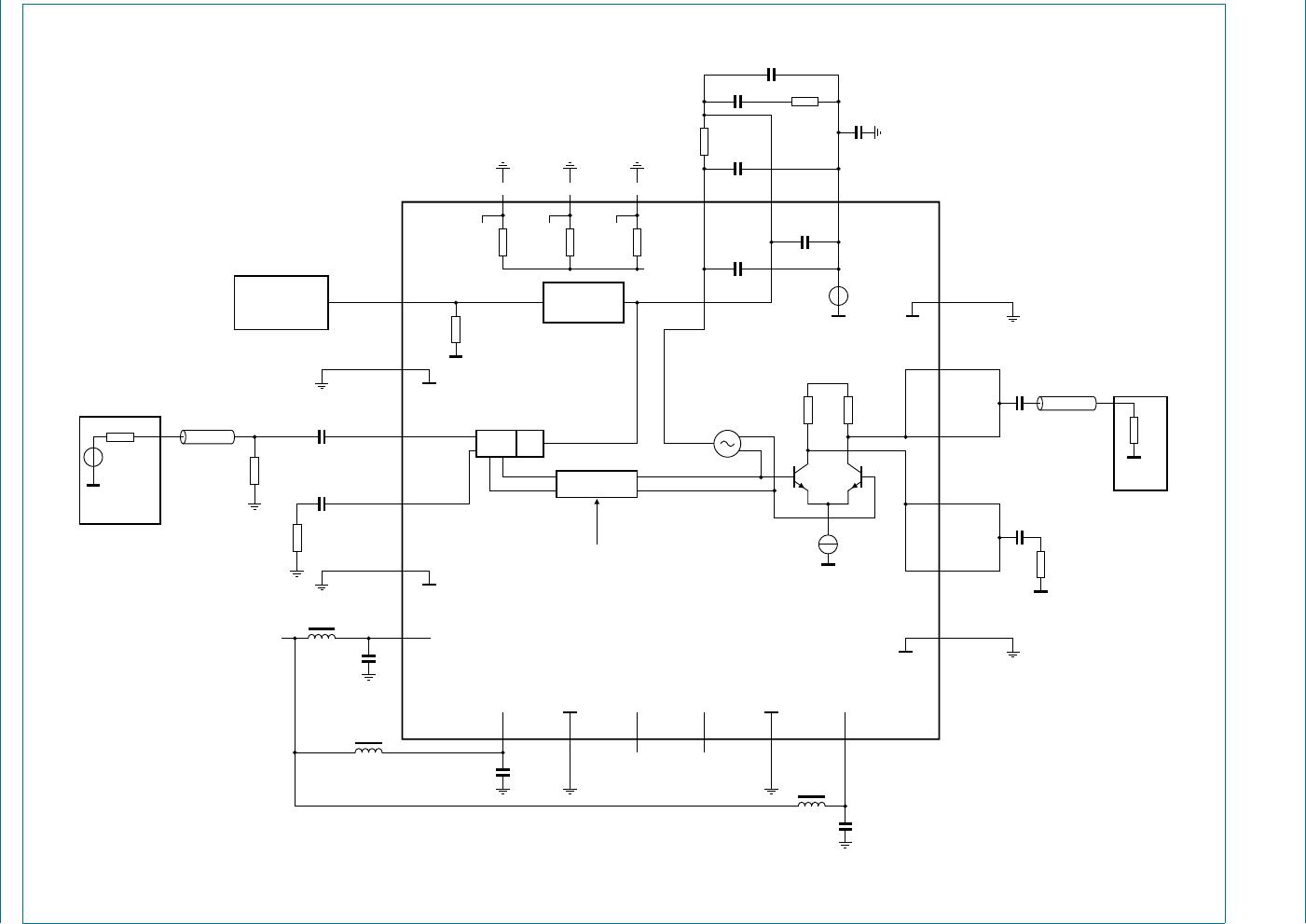
Low phase noise LO generator for VSAT applications
14. Characteristics
[1] The typical ratio of the maximum K
O
in relation to the minimum K
O
is 1.25.
[2] Output stage is a differential pair with 50 collector impedances.
Output power is measured per output pin for the fundamental tone only.
Output is DC coupled and is AC coupled in on-board.
Table 12. Characteristics
Operating conditions of Table 10 apply.
Symbol Parameter Conditions Min Typ Max Unit
V
CC
supply voltage 3.0 3.3 3.6 V
I
CC
supply current - 100 130 mA
PLL
f
o(RF)
RF output frequency 9.03 - 9.22 GHz
V
O(reg)VCO
VCO regulator output voltage 2.5 2.7 2.9 V
I
cp
charge pump current - 1 - mA
K
O
VCO steepness
[1]
- 0.48 - GHz/V
n(VCO)
VCO phase noise at 10 MHz offset - 130 - dBc/Hz
n(synth)
synthesizer phase noise divider value = 64; at 100 kHz
offset; reference phase noise is
149 dBc/Hz at 100 kHz offset
- 97 92 dBc/Hz
Output buffer
P
o
output power measured single ended
[2]
5- 1dBm
RL
out
output return loss measured at demo board and
de-embedded to footprint
- 10 - dB
sup(sp)ref
reference spurious suppression measured at divider value = 256 - - 70 dBc
H(LO)
LO harmonic rejection - 10 - dBc
Lock detector
V
OL
LOW-level output voltage I
O
= 1 mA - - 0.4 V
V
OH
HIGH-level output voltage I
O
= 1 mA 2.2 - - V
R
pd
pull-down resistance 70 100 130 k
Divider setting (NSL0, NSL1, NSL2)
R
pu
pull-up resistance 70 100 130 k
V
IL
LOW-level input voltage - - 0.8 V
V
IH
HIGH-level input voltage 2.0 - - V