TFF11092HN All information provided in this document is subject to legal disclaimers. © NXP B.V. 2013. All rights reserved.
Product data sheet Rev. 1 — 28 March 2013 7 of 17
NXP Semiconductors
TFF11092HN
Low phase noise LO generator for VSAT applications
LCKDET (pin 7) has a pull-down resistor of 100 k to GND1(REF) (pin 8).
10.4 Reference input (IN(REF)_P, IN(REF)_N)
The reference input is a differential pair and is internally biased. The input is high ohmic.
The input signal must be AC coupled. If used in a single ended mode, the not used input
must be terminated with the same impedance as the driving source.
An example of the differential source and two single ended loads are shown in Figure 7
.
An example of a single ended application is shown in Figure 8
.
Table 6. Logical value and physical value for lock detect (LCKDET)
Logical value Physical value Lock detect state
0 0 V out of lock
1 2.5 V lock
(1) The attack time and decay time are typically 10 s and are mainly depending on the drift of the VCO tuning voltage.
Fig 6. Timing diagram lock detector
001aal986
value determined
by closed loop
opertation PLL
VTUNE
LCKDET(t)
VTUNE(t)
IN(REF)_P/N(t)
Drift to maximum
voltage = lowest
frequency of
VCO
undetermined
behavior around
maximum
voltage
undetermined
behavior around
maximum
voltage
voltage is forced
by loop to closed
loop value of
PLL
value is determined by
closed loop operation
PLL
PLL is in lockactual PLL status PLL is out of lock PLL is out of lock PLL is out of lock PLL is in lock PLL is in lock
LCKDET > 2.2 V
remarks
LCKDET
remains > 2.2 V
because loop
filter is still
charged
window detector
detects that
VTUNE > upper
window detector
threshold.
LCKDET changes
from > 2.2 V to
< 0.4 V during the
attack time
LCKDET < 0.4 V window detector
detects that
VTUNE < upper
window detector
threshold 0.1 V.
LCKDET changes
from < 0.4 V to
> 2.2 V during the
decay time
LCKDET > 2.2 V
1timeline section
IN LOCK
2.2 V
low window detector threshold
(7% of V
O(reg)VCO
)
2345
attack time
(1)
decay time
(1)
6
t
t
t
0.4 V
OUT OF LOCK (0 V)
upper window detector threshold
(93% of V
O(reg)VCO
)
hysteresis voltage (0.1 V)
TFF11092HN All information provided in this document is subject to legal disclaimers. © NXP B.V. 2013. All rights reserved.
Product data sheet Rev. 1 — 28 March 2013 8 of 17
NXP Semiconductors
TFF11092HN
Low phase noise LO generator for VSAT applications
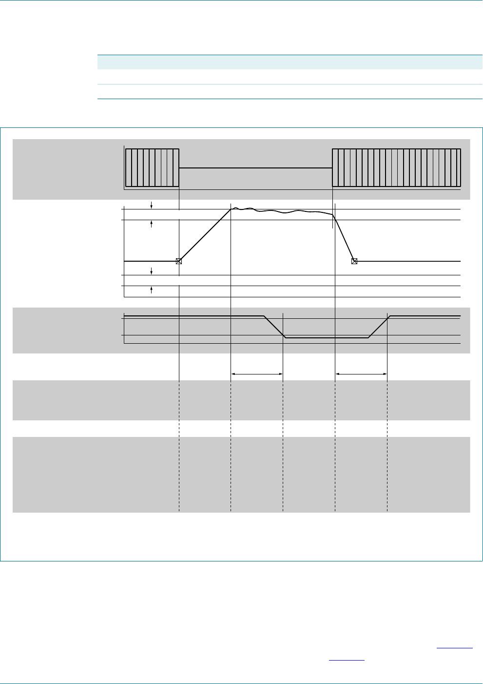
Note that the phase noise of the output signal is also determined by the phase noise of the
reference signal. The reference frequency range is equal to the
output frequency / division value. Note that the output frequency is guaranteed from
8.20 GHz to 8.60 GHz.
10.5 Divider settings (NSL2, NSL1, NSL0)
The divider can be set to 16, 32, 64, 128 and 256 (See Table 8). The logic levels for
NSL0 (pin 4), NSL1 (pin 5) and NSL2 (pin 6) are given in Table 7
.
The pins have a pull-up resistor of 100 k to V
CC(DIV)
(pin 13).
The device is only guaranteed when NSL2, NSL1 and NSL0 are predefined at start-up (no
change of divider value is allowed during operation).
The truth table is shown in Table 8.
[1] Test mode, divider output will be disabled.
11. Limiting values
Table 7. Logical and physical value for divider setting (NSL2, NSL1, NSL0)
Logical value Physical value
0GND
1 open or V
CC
Table 8. Divider setting as function of NSL2, NSL1 and NSL0
Setting number NSL2 NSL1 NSL0 Divider value
000016
100132
201064
3011128
4100256
5101
[1]
6110
[1]
7111
[1]
Table 9. Limiting values
In accordance with the Absolute Maximum Rating System (IEC 60134).
Symbol Parameter Conditions Min Max Unit
V
I
input voltage on pin NSL0 0.5 +5 V
on pin NSL1 0.5 +5 V
on pin NSL2 0.5 +5 V
on pin IN(REF)_P 0.5 +5 V
on pin IN(REF)_N 0.5 +5 V
on pin V
CC(REF)
0.5 +5 V
on pin V
CC(DIV)
0.5 +5 V
on pin V
CC(BUF)
0.5 +5 V
TFF11092HN All information provided in this document is subject to legal disclaimers. © NXP B.V. 2013. All rights reserved.
Product data sheet Rev. 1 — 28 March 2013 9 of 17
NXP Semiconductors
TFF11092HN
Low phase noise LO generator for VSAT applications
12. Recommended operating conditions
[1] Required reference phase noise is set 10 dB below equivalent input phase noise.
13. Thermal characteristics
P
i
input power on pin IN(REF)_P 4+10dBm
on pin IN(REF)_N 4+10dBm
T
j
junction temperature 40 +125 C
T
stg
storage temperature 40 +125 C
V
ESD
electrostatic discharge voltage Human Body Model (HBM);
According JEDEC standard
22-A114E
-2.5kV
Charged Device Model (CDM);
According to JEDEC standard
22-C101B
-1kV
Table 9. Limiting values
…continued
In accordance with the Absolute Maximum Rating System (IEC 60134).
Symbol Parameter Conditions Min Max Unit
Table 10. Operating conditions
NSL0 (pin 4), NSL1 (pin 5) and NSL2 (pin 6) not changed during operation.
Loop filter component values as depicted in Table 5
are used.
Symbol Parameter Conditions Min Typ Max Unit
T
amb
ambient temperature 40 +25 +85 C
Z
0
characteristic impedance - 50 -
n(ref)
reference phase noise divider value = 16
[1]
--134 dBc/Hz
divider value = 32
[1]
--143 dBc/Hz
divider value = 64
[1]
--149 dBc/Hz
divider value = 128
[1]
--150 dBc/Hz
divider value = 256
[1]
--151 dBc/Hz
f
i(ref)
reference input frequency f
i(ref)
= f
o(RF)
/ divider value 35 - 576 MHz
P
i(ref)
reference input power 10 - 0 dBm
Table 11. Thermal characteristics
Symbol Parameter Conditions Typ Unit
R
th(j-sp)
thermal resistance from junction to solder point 25 K/W

TFF11092HN/N1X

Mfr. #:
Manufacturer:
NXP Semiconductors
Description:
Phase Locked Loops - PLL Low phase noise LO generator forVSAT
Lifecycle:
New from this manufacturer.
Delivery:
DHL FedEx Ups TNT EMS
Payment:
T/T Paypal Visa MoneyGram Western Union

Products related to this Datasheet