NJM2211
-1-
Ver.2003-12-09
FSK DEMODULATOR / TONE DECODER
■ GENERAL DESCRIPTION ■ PACKAGE OUTLINE
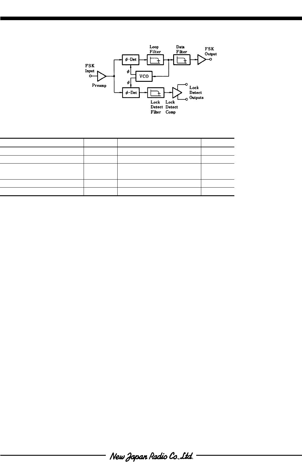
The NJM2211 is a monolithic phase-locked loop (PLL) system especially
designed for data communications. It is particularly well suited for FSK modem
applications, and operates over a wide frequency range of 0.01Hz to 300kHz. It
can accommodate analog signals between 2mV and 3V, and can interface with
conventional DTL, TTL and ECL logic families. The circuit consists of a basic
PLL for tracking an input signal frequency within the passband, a quadrature
phase detector which provides carrier detection, and an FSK voltage
comparator which provides FSK demodulation. External components are used
to independently set carrier frequency, bandwidth, and output delay.
■ FEATURES
● Wide Operating Voltage (4.5V to 20V)
● Wide frequency range (0.01Hz to 300kHz)
● DTL / TTL / ECL logic compatibility
● FSK demodulation with carrier-detector
● Wide dynamic range (2mV to 3V
rms
)
● Adjustable tracking range (±1% to ±80%)
● Excellent temperature stability (20ppm / °C typical)
● Package Outline DIP14, DMP14
● Bipolar Technology
■ APPLICATIONS
● FSK demodulation
● Data synchronization
● Tone decoding
● FM detection
● Carrier detection
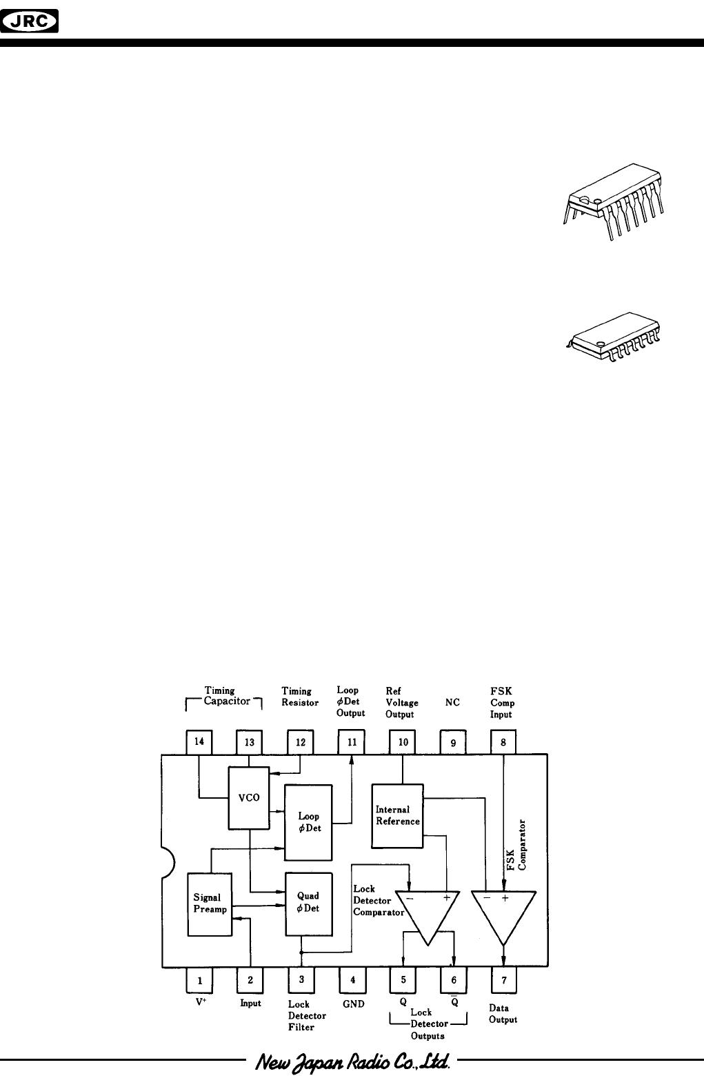
■ PIN CONFIGURATION
NJM2211D
NJM2211M
NJM2211D
NJM2211M