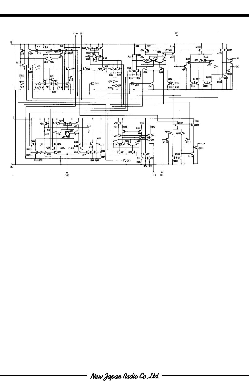
NJM2211
- 4 -
Ver.2003-12-09
EQUIVALENT CIRCUIT
CIRCUIT FUNCTION
Signal Input (Pin 2)
The input signal is AC coupled to this terminal. The internal impedance at pin 2 is 20k, Recommended input signal
leveles in the range of 10mVrms to 3Vrms.
Quadrature Phase Detector Output (Pin 3)
This is the high-impedance output of the quadrature phase detector, and is internally connected to the input of lock-detect
voltage comparator. In tone detection applications, pin 3 is connected to ground through a parallel combination of R
D
and
C
D
(see Figure 1) to eliminate chatter at the lock-detect outputs. If this tone-detect section is not used, pin 3 can be left
open circuited.
Lock-Detect Output, Q (Pin 5)
The output at pin 5 is at a "high" state when the PLL is out of lock and goes to a "low" or conducting state when the PLL is
locked. It is an open collector type output and required a pull-up resistor, R
L
, to V
+
for proper operation. In the "low" state it
can sink up to 5mA of load current.
Lock-Detect Complement, Q (Pin 6)
The output at pin 6 is the logic complement of the lock-detect output at pin 5. This output is also an open collector type
stage which can sink 5mA of load current in the low or "on" state.
FSK Data Output (Pin 7)
This output is an open collector logic stage which requres a pull-up resistor, R
L
, to V
+
for proper operation. It can sink 5mA
of load current. When decoding FSK signals the FSK data output will switch to a "high"or off state for low input frequency,
and will switch to a "low" or on state for high input frequency. If no input signal is present, the logic state at pin 7 is
indeterminate.
FSK Comparator Input (Pin 8)
This is the high-impedance input to the FSK voltage comparator. Normally, an FSK post-detection or data filter is
connected between this terminal and the PLL phase-detector output (pin 11). This data filter is formed by R
F
and C
F
of
Figure 1. The threshold voltage of the comparator is set by the internal reference voltage, V
R
, available at pin 10.
NJM2211
-
5
-
Ver.2003-12-09
Reference Voltage V
R
(Pin 10)
This pin is internally biased at the reference voltage level, V
R
; V
R
=V+ / 2-650mV. The DC voltage level at this pin forms
an internal reference for the voltage levels at pin 3, 8, 11, and 12. Pin 10 must be bypassed to ground with a 0.1µF
capacitor.
Loop Phase Detector Output (Pin 11)
This terminal provides a high impedance output for the loop phase-detector. The PLL loop filter is formed by R1 and C1
connected to pin 11 (see Figure 1). With no input signal, or with no phase error within the PLL, the DC level at pin 11 is
very nearly equal to V
REF
. The peak voltage swing available at the phase detector output is equal to ±V
REF
.
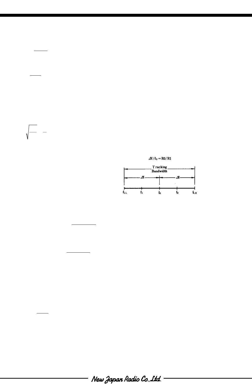
Figure 1. FSK & Tone Detection
VCO Control Input (Pin 12)
VCO free-running frequency is determined by external timing resistor, R0, connected from this terminal to ground. The
VCO free-running frequency, f
0
, is given by :
()
0C0R
1
Hzf
0
=
where C0 is the timing capacitor across pins 13 and 14. For optimum temperature stability R0 must be in the range of
10k to 100k (see Typical Electrical Characteristics).
This terminal is a low impedance point, and is internally biased at a DC level equal to V
R
. The maximum timing current
drawn from pin 12 must be limited to 3mA for proper operation of the circuit.
VCO Timing Capacitor (Pins 13 and 14)
VCO frequency is inversely proportional to the external timing capacitor, C0, connected across these terminals. C0 must
be non-polarized, and in the range of 200pF to 10µF.
VCO Frequency Adjustment
VCO can be fine tuned by connecting a potentiometer, R
X
, in series with R0 at pin 12 (see Figure 2)
VCO Free-Running Frequency, F
0
The NJM2211 does not have a separate VCO output terminal. Instead, the VCO outputs are internally connected to the
phase-detector sections of the circuit. However, for setup or adjustment purposes, the VCO free-running frequency can
be measured at pin 3 (with C
D
disconnected) with no input and also pin 2 shorted to pin 10.
NJM2211
-
6
-
Ver.2003-12-09
DESIGN EQUATIONS
See Figure 1 for Definitions of Components.
1. VCO Center Frequency, f
0
:
()
0C0R
1
Hzf
0
=
2. Internal Reference Voltage, V
R
(measured at pin 10) :
mV650
2
V
V
S
R
+
=
3. Loop Lowpass Filter Time Constant, τ :
τ=R1C1
4. Loop Damping, ξ :
=
4
1
C
C
ξ
1
0
5. Loop Tracking Bandwidth, ±f/f
0
:
f/f
0
=R0 / R1
6. FSK Date Filter Time Constant, τ
F
:
τ
F
=R
F
C
F
7. Loop Phase Detector Conversion Gain, K
φ
:
(K
φ
is the differential DC voltage across pins 10 and 11, per unit of phase error at phase-detector input) :
(
)
(
)
π
V2
radian) per volts (in K
REF
φ
=
8. VCO conversion Gain, K
0
, is the amount of change in VCO frequency per unit of DC voltage change at pin 11 :
REF
0
V1R0C
1
volt) per Hertz (in K
=
9. Total Loop Gain K
τ
:
K
T
(in radians per second per volt =2πKφK
0
=4 / C
0
R
1
10. Peak Phase-Detector Current, I
A
:
25
V
)mA(I
REF
A
=

NJM2211M

Mfr. #:
Manufacturer:
NJR (New Japan Radio)
Description:
Modulator / Demodulator Demodulator/Decoder
Lifecycle:
New from this manufacturer.
Delivery:
DHL FedEx Ups TNT EMS
Payment:
T/T Paypal Visa MoneyGram Western Union

Products related to this Datasheet