FEDR44V064B-02
Issue Date: Sep. 07, 2017
MR44V064B
64k Bit(8,192-Word × 8-Bit) FeRAM (Ferroelectric Random Access Memory) I2C
1/16
GENERAL DESCRIPTION
The MR44V064B is a nonvolatile 8,192-word x 8-bit ferroelectric random access memory (FeRAM) developed
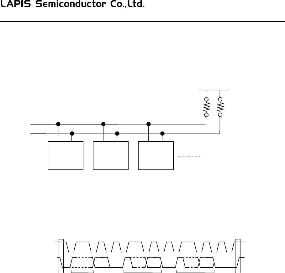
in the ferroelectric process and silicon-gate CMOS technology. The MR44V064B is accessed using Two-wire
Serial Interface ( I2C BUS ).Unlike SRAMs, this device, whose cells are nonvolatile, eliminates battery backup
required to hold data. This device has no mechanisms of erasing and programming memory cells and blocks,
such as those used for various EEPROMs. Therefore, the write cycle time can be equal to the read cycle time and
the power consumption during a write can be reduced significantly.
The MR44V064B can be used in various applications, because the device is guaranteed for the write/read
tolerance of 10
12
cycles per bit and the rewrite count can be extended significantly.
FEATURES
• 8,192-word × 8-bit configuration I2C BUS Interface
A single 3.3 V typ (1.8V to 3.6V) power supply
• Operating frequency: 3.4MHz(Max) HS-mode
1MHz(Max) F/S-mode Plus
• Read/write tolerance 10
12
cycles/bit
Data retention 10 years
Guaranteed operating temperature range 40 to 85°C
• Package options:
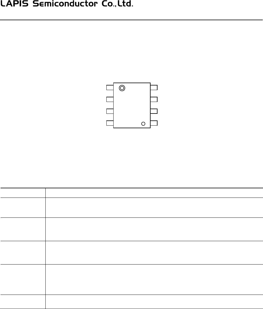
8-pin plastic SOP (P-SOP8-200-1.27-T2K)
RoHS (Restriction of hazardous substances) compliant
FEDR44V064B-02
MR44V064B
2/16
PIN CONFIGURATION
PIN DESCRIPTIONS
Pin Name
Description
A0 – A2
Address ( input )
Address pin indicates device address. When Address value is match the device address
code from SDA, the device will be selected. The address pins are pulled down internally.
SDA
Serial data input serial data output ( input / output )
SDA is a bi-directional line for I2C interface. The output driver is open-drain. A pull-up
resistor is required.
SCL
Serial Clock ( input )
Serial Clock is the clock input pin for setting for serial data timing. Inputs are latched on
the rising edge and outputs occur on the falling edge.
WP
Write protect ( input )
Write Protect pin controls write-operation to the memory. When WP is high, all address in
the memory will be protected. When WP is low, all address in the memory will be written.
WP pin is pulled down internally.
V
CC
, V
SS
Power supply
Apply the specified voltage to V
CC
. Connect V
SS
to ground.
8-pin plastic SOP
A0
A1
A2
VSS
VCC
WP
SCL
SDA
1 8
2 7
3 6
4 5
MR44V064B
FEDR44V064B-02
MR44V064B
3/16
I2C BUS
The MR44V064B employs a bi-directional two-wire I2C BUS interface, works as a slave device.
An example of I2C interface system with MR44V064B
I2C BUS COMUNICATION
I2C BUS data communication starts by start condition input, and ends by stop condition input. Data is always
8bit long, acknowledge is always required after each byte. I2C BUS carries out data transmission with plural
devices connected by 2 communication lines of serial data ( SDA ) and serial clock ( SCL ).
START CONDITION
Before executing each command, start condition ( start bit ) where SDA goes from “HIGH” down to “LOW”
when SCL is “HIGH” is necessary. MR44V064B always detects whether SDA and SCL are in start condition
( start bit ) or not, therefore, unless this condition is satisfied, any command is executed.
STOP CONDITION
Each command can be ended by SDA rising from “LOW” to “HIGH” when stop condition ( stop bit ),
namely,SCL is “HIGH”.
SCL
SDA
START
condition
1-7 8 9 1-7 8 9 1-7 8 9
STOP
condition
ADDRESS R/W ACK DATA ACK
DATA ACK
SCL
SDA
Pull-up
resistor
SCL SDA
I2C BUS
master
SCL SDA
MR44V064B
(slave)
A2 A1 A0
0 0 0
SCL SDA
MR44V064B
(slave)
A2 A1 A0
0 0 1

MR44V064BMAZAATL

Mfr. #:
Manufacturer:
Description:
F-RAM FeRAM/64Kbit 8Kb x 8 8pin SOP 3.4MHz
Lifecycle:
New from this manufacturer.
Delivery:
DHL FedEx Ups TNT EMS
Payment:
T/T Paypal Visa MoneyGram Western Union

Products related to this Datasheet